XE8000EV101 Semtech, XE8000EV101 Datasheet - Page 4
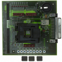
XE8000EV101
Manufacturer Part Number
XE8000EV101
Description
EVAL BOARD FOR XE8801AMI027LF
Manufacturer
Semtech
Type
MCUr
Specifications of XE8000EV101
Contents
Fully Assembled Evaluation Board
For Use With/related Products
XE88LC01AMI027
Lead Free Status / RoHS Status
Contains lead / RoHS non-compliant


XE8801A – SX8801R
1.1 Top schematic
1.1.1 General description
The top level block schematic of the circuit is shown in Figure 1-1. The heart of the circuit consists of the
Coolrisc816® CPU core. This core includes an 8x8 multiplier and 16 internal registers.
The bus controller generates all control signals for access to all data registers other than the CPU internal
registers.
The reset block generates the adequate reset signals for the rest of the circuit as a function of the set-up contained
in its control registers. Possible reset sources are the power-on-reset (POR), the external pin RESET, the
watchdog (WD), a bus error detected by the bus controller or a programmable pattern on Port A. Different low
power modes are implemented.
The clock generation and power management block sets up the clock signals and generates internal supplies for
different blocks. The clock can be generated from the RC oscillator (this is the start-up condition), the crystal
oscillator (XTAL) or an external clock source (given on the OSCIN pin).
The test controller generates all set-up signals for different test modes. In normal operation, it is used as a set of 8
low power data registers. If power consumption is important for the application, the variables that need to be
accessed very often should be stored in these registers rather than in the RAM.
The IRQ handler routes the interrupt signals of the different peripherals to the IRQ inputs of the CPU core. It allows
masking of the interrupt sources and it flags which interrupt source is active.
Events are generally used to restart the processor after a HALT period without jumping to a specified address, i.e.
the program execution resumes with the instruction following the HALT instruction. The EVN handler routes the
event signals of the different peripherals to the EVN inputs of the CPU core. It allows masking of the interrupt
sources and it flags which interrupt source is active.
The Port B is an 8 bit parallel IO port with analog capabilities. The URST, UART, and PWM block also make use of
this port.
The instruction memory is a 22-bit wide flash or ROM memory depending on the circuit version. Flash and ROM
versions have both 8k instruction memory.
The data memory on this product is a 512 byte SRAM.
The Acquisition Chain is a high resolution acquisition path with the 16+10 bits ZoomingADC™. The VMULT
(voltage multiplier) powers a part of the Acquisition Chain.
Port A is an 8 bit parallel input port. It can also generate interrupts, events or a reset. It can be used to input
external clocks for the timer/counter/PWM block.
Port C is a general purpose 8 bit parallel I/O port.
The USRT (universal synchronous receiver/transmitter) contains some simple hardware functions in order to
simplify the software implementation of a synchronous serial link.
The UART (universal asynchronous receiver/transmitter) contains a full hardware implementation of the
asynchronous serial link.
© Semtech 2005
www.semtech.com
1-2
Related parts for XE8000EV101
Image
Part Number
Description
Manufacturer
Datasheet
Request
R

Part Number:
Description:
EVALUATION BOARD
Manufacturer:
Semtech
Datasheet:
Part Number:
Description:
EVALUATION BOARD
Manufacturer:
Semtech
Datasheet:
Part Number:
Description:
VOLTAGE SUPPRESSOR, TRANSIENT SEMTECH
Manufacturer:
Semtech
Datasheet:

Part Number:
Description:
HIGH VOLTAGE CAPACITORS MONOLITHIC CERAMIC TYPE
Manufacturer:
Semtech Corporation
Datasheet:
Part Number:
Description:
EZ1084CM5.0 AMP POSITIVE VOLTAGE REGULATOR
Manufacturer:
Semtech Corporation
Datasheet:
Part Number:
Description:
3.0 AMP LOW DROPOUT POSITIVE VOLTAGE REGULATORS
Manufacturer:
Semtech Corporation
Datasheet:
Part Number:
Description:
Manufacturer:
Semtech Corporation
Datasheet:
Part Number:
Description:
RailClamp Low Capacitance TVS Diode Array
Manufacturer:
Semtech Corporation
Datasheet:
Part Number:
Description:
Manufacturer:
Semtech Corporation
Datasheet:
Part Number:
Description:
Manufacturer:
Semtech Corporation
Datasheet:
Part Number:
Description:
Manufacturer:
Semtech Corporation
Datasheet:
Part Number:
Description:
Manufacturer:
Semtech Corporation
Datasheet: