AD8364-EVAL-2140 Analog Devices Inc, AD8364-EVAL-2140 Datasheet - Page 24
AD8364-EVAL-2140
Manufacturer Part Number
AD8364-EVAL-2140
Description
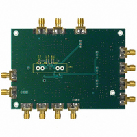
BOARD EVAL AD8364 2140MHZ
Manufacturer
Analog Devices Inc
Datasheet
1.AD8364-EVAL-2140.pdf
(48 pages)
Specifications of AD8364-EVAL-2140
Module/board Type
Evaluation Board
For Use With/related Products
AD8364 2.140GHz only
Lead Free Status / RoHS Status
Contains lead / RoHS non-compliant


AD8364
CONTROLLER MODE BASIC CONNECTIONS
In addition to being a measurement device, the AD8364 can
also be configured to measure and control rms signal levels. The
AD8364 has two controller modes. Each of the two rms log
detectors can be separately configured to set and control the
output power level of a variable gain amplifier (VGA) or
variable voltage attenuator (VVA). Alternatively, the two rms
log detectors can be configured to measure and control the gain
of an amplifier or signal chain.
Automatic Power Control
Figure 61 shows how the device should be reconfigured to
control output power.
The RF input to the device is configured as before. A directional
coupler taps off some of the power being generated by the VGA
(typically a 10 dB to 20 dB coupler is used). A power splitter can
be used instead of a directional coupler if there are no concerns
about reflected energy from the next stage in the signal chain.
Some additional attenuation may be required to set the
maximum input signal at the AD8364 to be equal to the
INPB
INPA
0.1µF
0.1µF
C5
C2
1:4
1:4
T1
T2
100pF
0.1µF
C11
C10
0.1µF
0.1µF
0.1µF
0.1µF
Figure 60. Basic Connections for Operation in Measurement Mode
C7
C6
C4
C3
VPOS
VPOS
C20
100pF
C21
0.1µF
25
26
27
28
29
30
31
32
0.1µF
0.1µF
0.1µF
0.1µF
VPSA
INHA
INLA
PWDN
COMR
INLB
INHB
VPSB
C22
C9
C9
100pF
C1
CHPA
CHPB
C23
24
1
Rev. 0 | Page 24 of 48
DECA
DECB
23
2
C24
100pF
COMA
COMB
C8
0.1µF
22
3
AD8364ACPZ
R19
R24
EXPOSED PADDLE
0Ω
R5
0Ω
VPOS
VPSR
ADJB
1
recommended maximum input level for optimum linearity and
temperature stability at the frequency of operation.
VSTA and OUTA are no longer shorted together. OUTA now
provides a bias or gain control voltage to the VGA. The gain
control sense of the VGA must be negative and monotonic, that
is, increasing voltage tends to decrease gain. However, the gain
control transfer function of the device does not need to be well
controlled or particularly linear. If the gain control sense of the
VGA is positive, an inverting op amp circuit with a dc offset
shift can be used between the AD8364 and the VGA to keep the
gain control voltage in the 0 V to 5 V range.
VSTA becomes the setpoint input to the system. This can be
driven by a DAC, as shown in Figure 61, if the output power is
expected to vary, or it can simply be driven by a stable reference
voltage if constant output power is required. This DAC should
have an output swing that covers the 0 V to 3.5 V range. The
AD7391
DACs provide adequate resolution (4 mV/bit) and an output
swing up to 4.5 V.
21
4
1
R20
SEE TEXT.
ACOM
ADJA
1
20
5
C13
0.1µF
C12
100pF
R18
R17
and
TEMP
VREF
1
1
19
6
0.1µF
C19
AD7393
ACOM
VLVL
18
7
CLPB
CLPA
17
8
OUTN
OUTB
OUTA
FBKA
OUTP
FBKB
VSTB
serial-input and parallel-input 10-bit
VSTA
C16
0.1µF
C14
0.1µF
16
15
14
13
12
11
10
9
OUTA
OUTP
OUTN
OUTB
Related parts for AD8364-EVAL-2140
Image
Part Number
Description
Manufacturer
Datasheet
Request
R

Part Number:
Description:
LF to 2.7GHz, Dual 60dB TruPwr™ Detector; Package: EVALUATION BOARDS; No of Pins: -; Temperature Range: Commercial
Manufacturer:
Analog Devices
Datasheet:
Part Number:
Description:
LF to 2.7GHz, Dual 60dB TruPwr Detector
Manufacturer:
Analog Devices
Datasheet:

Part Number:
Description:
±1.7g Dual-Axis IMEMS Accelerometer Evaluation Board
Manufacturer:
Analog Devices Inc
Datasheet:

Part Number:
Description:
Inertial Sensor Evaluation System
Manufacturer:
Analog Devices Inc
Datasheet:
Part Number:
Description:
Manufacturer:
Analog Devices Inc
Datasheet:
Part Number:
Description:
Manufacturer:
Analog Devices Inc
Datasheet:
Part Number:
Description:
Manufacturer:
Analog Devices Inc
Datasheet:
Part Number:
Description:
Manufacturer:
Analog Devices Inc
Datasheet:
Part Number:
Description:
Manufacturer:
Analog Devices Inc
Datasheet:
Part Number:
Description:
Manufacturer:
Analog Devices Inc
Datasheet:
Part Number:
Description:
Manufacturer:
Analog Devices Inc
Datasheet:
Part Number:
Description:
Manufacturer:
Analog Devices Inc
Datasheet:
Part Number:
Description:
Manufacturer:
Analog Devices Inc
Datasheet: