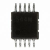
RCLAMP0544M.TBT Semtech, RCLAMP0544M.TBT Datasheet - Page 5

RCLAMP0544M.TBT
Manufacturer Part Number
RCLAMP0544M.TBT
Description
IC TVS ARRAY FOR HDMI 10-MSOP
Manufacturer
Semtech
Series
RailClamp®r
Datasheet
1.RCLAMP0544M.TBT.pdf
(11 pages)
Specifications of RCLAMP0544M.TBT
Mfg Application Notes
TVS Diode AppNote SI04-14
Voltage - Reverse Standoff (typ)
5V
Voltage - Breakdown
6V
Polarization
4 Channel Array - Unidirectional
Mounting Type
Surface Mount
Package / Case
10-MSOP, Micro10™, 10-uMAX, 10-uSOP
Lead Free Status / RoHS Status
Lead free / RoHS Compliant
Power (watts)
-
Lead Free Status / Rohs Status
Compliant
Other names
RCLAMP0544MTR
Available stocks
Company
Part Number
Manufacturer
Quantity
Price
Part Number:
RCLAMP0544M.TBT
Manufacturer:
SEMTECH/美国升特
Quantity:
20 000
Device Connection Options for Protection of Four
High-Speed Data Lines
The RClamp0544M TVS is designed to protect four data
lines from transient over-voltages by clamping them to a
fixed reference. When the voltage on the protected line
exceeds the reference voltage (plus diode V
diodes are forward biased, conducting the transient
current away from the sensitive circuitry.
Flow Through Layout
The RClamp0544M is designed for have ease of PCB
layout by allowing the traces to run straight through the
device. Figure 1 shows the proper way to design the PCB
board trace in order to use the flow through layout for
two line pairs. The solid line represents the PCB trace.
Note that the PCB traces are used to connect the pin
pairs for each line (pin 1 to pin 10, pin 2 to pin 9, pin 4
to pin 7, pin 5 to pin 6). For example, line 1 enters at
pin 1 and exits at Pin 10 and the PCB trace connects pin
1 and 10 together. This is true for lines 2, 3, and 4.
Ground is connected at pin 3. This pin should be
connected directly to a ground plane on the board for
best results. The path length is kept as short as
possible to minimize parasitic inductance.
Circuit Board Layout Recommendations for Suppres-
sion of ESD.
Good circuit board layout is critical for the suppression of
ESD induced transients. The following guidelines are
recommended:
PROTECTION PRODUCTS
Applications Information
2006 Semtech Corp.
Place the device near the input terminals or connec-
tors to restrict transient coupling.
Minimize the path length between the TVS and the
protected line.
Minimize all conductive loops including power and
ground loops.
The ESD transient return path to ground should be
kept as short as possible.
Never run critical signals near board edges.
Use ground planes whenever possible.
F
) the steering
5
Matte Tin Lead Finish
Matte tin has become the industry standard lead-free
replacement for SnPb lead finishes. A matte tin finish is
composed of 100% tin solder with large grains. Since
the solder volume on the leads is small compared to the
solder paste volume that is placed on the land pattern of
the PCB, the reflow profile will be determined by the
requirements of the solder paste. Therefore, these
devices are compatible with both lead-free and SnPb
assembly techniques. In addition, unlike other lead-free
compositions, matte tin does not have any added alloys
that can cause degradation of the solder joint.
Figure 1. Flow through Layout for two Line Pairs
Figure 1. Flow through Layout for two Line Pairs
Figure 1. Flow through Layout for two Line Pairs
Figure 1. Flow through Layout for two Line Pairs
Figure 1. Flow through Layout for two Line Pairs
Line 1
Line 2
Gnd
Line 3
Line 4
1
RClamp0544M
PRELIMINARY
www.semtech.com
NC
Line 1
Line 2
Line 3
Line 4


