ESD9X3.3ST5G ON Semiconductor, ESD9X3.3ST5G Datasheet

TVS ESD ASD 102W 3.3V SOD-923

ESD9X3.3ST5G

Manufacturer Part Number
ESD9X3.3ST5G
Description
TVS ESD ASD 102W 3.3V SOD-923
Manufacturer
ON Semiconductor
Datasheet

Specifications of ESD9X3.3ST5G

Voltage - Reverse Standoff (typ)
3.3V
Voltage - Breakdown
5V
Power (watts)
102W
Polarization
Unidirectional
Mounting Type
Surface Mount
Package / Case
SOD-923
Lead Free Status / RoHS Status
Lead free / RoHS Compliant
Other names
ESD9X3.3ST5G
ESD9X3.3ST5GOSTR

Available stocks

Company
Part Number
Manufacturer
Quantity
Price
Part Number:
ESD9X3.3ST5G
Manufacturer:
ON Semiconductor
Quantity:
81 509
Part Number:
ESD9X3.3ST5G
Manufacturer:
ON
Quantity:
30 000
Part Number:
ESD9X3.3ST5G
Manufacturer:
ON
Quantity:
30 000
Part Number:
ESD9X3.3ST5G
Manufacturer:
ON
Quantity:
4 849
Part Number:
ESD9X3.3ST5G
Manufacturer:
ST
0
Part Number:
ESD9X3.3ST5G
Manufacturer:
ON/安森美
Quantity:
20 000
Part Number:
ESD9X3.3ST5G
0
Company:
Part Number:
ESD9X3.3ST5G
Quantity:
1 088 000
Company:
Part Number:
ESD9X3.3ST5G
Quantity:
300
ESD9X3.3ST5G SERIES
Transient Voltage
Suppressors
Micro−Packaged Diodes for ESD Protection
components from ESD. Excellent clamping capability, low leakage,
and fast response time provide best in class protection on designs that
are exposed to ESD. Because of its small size, it is suited for use in
cellular phones, MP3 players, digital cameras and many other portable
applications where board space is at a premium.
Specification Features:
Mechanical Characteristics:
CASE:
Epoxy Meets UL 94 V−0
LEAD FINISH:
MOUNTING POSITION:
QUALIFIED MAX REFLOW TEMPERATURE:
Device Meets MSL 1 Requirements
Stresses exceeding Maximum Ratings may damage the device. Maximum
Ratings are stress ratings only. Functional operation above the Recommended
Operating Conditions is not implied. Extended exposure to stresses above the
Recommended Operating Conditions may affect device reliability.
1. FR−5 = 1.0 x 0.75 x 0.62 in.
See Application Note AND8308/D for further description of survivability specs.
© Semiconductor Components Industries, LLC, 2008
August, 2008 − Rev. 6
MAXIMUM RATINGS
IEC 61000−4−2 (ESD)
ESD Voltage
Total Power Dissipation on FR−5 Board
Junction and Storage Temperature Range
Lead Solder Temperature − Maximum
The ESD9X Series is designed to protect voltage sensitive
Low Clamping Voltage
Small Body Outline Dimensions:
Low Body Height: 0.017″ (0.43 mm) Max
Stand−off Voltage: 3.3 V − 12 V
Low Leakage
Response Time is Typically < 1 ns
ESD Rating of Class 3 (> 16 kV) per Human Body Model
IEC61000−4−2 Level 4 ESD Protection
These are Pb−Free Devices
(Note 1) @ T
(10 Second Duration)
Void-free, transfer-molded, thermosetting plastic
0.039″ x 0.024″ (1.0 mm x 0.60 mm)
100% Matte Sn (Tin)
A
Rating
= 25°C
Per Human Body Model
Per Machine Model
Any
Contact
Air
Symbol
T
J
P
, T
T
D
L
stg
260°C
−55 to
Value
+150
±30
±30
400
150
260
16
1
Unit
mW
kV
kV
°C
°C
V
†For information on tape and reel specifications,
ESD9XxxST5G
See specific marking information in the device marking
column of the table on page 2 of this data sheet.
including part orientation and tape sizes, please
refer to our Tape and Reel Packaging Specifications
Brochure, BRD8011/D.
Device
CASE 514AA
DEVICE MARKING INFORMATION
SOD−923
ORDERING INFORMATION
X
M
1
http://onsemi.com
PIN 1. CATHODE
= Specific Device Code
= Date Code
SOD−923
Package
2. ANODE
Publication Order Number:
8000/Tape & Reel
ESD9X3.3ST5G/D
MARKING
DIAGRAM
2
Shipping
X M

Related parts for ESD9X3.3ST5G

ESD9X3.3ST5G Summary of contents

Page 1

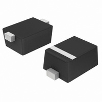
... ESD9X3.3ST5G SERIES Transient Voltage Suppressors Micro−Packaged Diodes for ESD Protection The ESD9X Series is designed to protect voltage sensitive components from ESD. Excellent clamping capability, low leakage, and fast response time provide best in class protection on designs that are exposed to ESD. Because of its small size suited for use in cellular phones, MP3 players, digital cameras and many other portable applications where board space premium ...

Page 2

... Max. Capacitance @ and MHz R *See Application Note AND8308/D for detailed explanations of datasheet parameters. ELECTRICAL CHARACTERISTICS V I RWM ( Device Marking Max Device* ESD9X3.3ST5G A 3.3 ESD9X5.0ST5G B 5.0 ESD9X7.0ST5G 5** 7.0 ESD9X12ST5G C 12 *Other voltages available upon request. **Rotated 270 degrees measured with a pulse test current ...

Page 3

... ON Semiconductor has developed a way to examine the entire voltage waveform across the ESD protection diode over the time domain of an ESD pulse in the form of an oscilloscope screenshot, which can be found on the datasheets for all ESD protection diodes ...

Page 4

TEMPERATURE (°C) Figure 6. Typical Breakdown Voltage versus Temperature TYPICAL CHARACTERISTICS 150 −55 ...

Page 5

... E 0.55 0.60 0.65 0.022 0.024 0.026 H 0.95 1.00 1.05 0.037 0.039 0.041 E L 0.05 0.10 0.15 0.002 0.004 0.006 ON Semiconductor Website: www.onsemi.com Order Literature: http://www.onsemi.com/orderlit For additional information, please contact your local Sales Representative ESD9X3.3ST5G/D ...

Related keywords