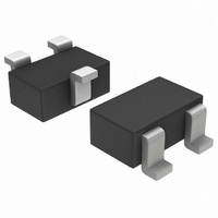
DF3A6.8FUT1
Zener Transient Voltage
Suppressor
Dual Common Anode Zeners for ESD
Protection
applications requiring transient overvoltage protection capability. They
are intended for use in voltage and ESD sensitive equipment such as
computers, printers, business machines, communication systems,
medical equipment and other applications. Their dual junction common
anode design protects two separate lines using only one package. These
devices are ideal for situations where board space is at a premium.
Features
Mechanical Characteristics
1. Mounted on FR−5 Board = 1.0 X 0.75 X 0.062 in.
2. Non−repetitive pulse per Figure 1.
3. Non−repetitive pulse per Figure 2.
July, 2004 − Rev. 1
MAXIMUM RATINGS
Maximum ratings are those values beyond which device damage can occur.
Maximum ratings applied to the device are individual stress limit values (not
normal operating conditions) and are not valid simultaneously. If these limits
are exceeded, device functional operation is not implied, damage may occur
and reliability may be affected.
Steady State Power Dissipation
Thermal Resistance Junction−to−Ambient
Operating Junction and Storage
Peak Power Dissipation @ 1.0 ms
Peak Power Dissipation @ 20 ms (Note 3)
ESD Discharge
These dual monolithic silicon zener diodes are designed for
Pb−Free Package is Available
SC−70 Package Allows Two Separate Unidirectional Configurations
Low Leakage < 1.0 mA @ 5.0 V
Breakdown Voltage: 6.4−7.2 V @ 5.0 mA
ESD Protection Meeting:16 kV Human Body Model
Peak Power: 24 W @ 1.0 ms (Unidirectional), per Figure 1
Peak Power: 150 W @ 20 ms (Unidirectional), per Figure 2
Void Free, Transfer−Molded, Thermosetting Plastic Case
Corrosion Resistant Finish, Easily Solderable
Package Designed for Optimal Automated Board Assembly
Small Package Size for High Density Applications
Semiconductor Components Industries, LLC, 2004
Derate above 25 C (Note 1)
Temperature Range
(Note 2) @ T
@ T
MIL STD 883C − Method 3015−6
IEC61000−4−2, Air Discharge
IEC61000−4−2, Contact Discharge
A
= 25 C
A
= 25 C
Rating
Preferred Device
30 kV Contact = IEC61000−4−2
Symbol
T
R
J
P
P
V
P
, T
qJA
PK
PK
PP
D
stg
− 55 to
Value
+150
200
618
150
1.6
20
16
30
30
mW/ C
1
Unit
mW
C/W
kV
W
W
C
†For information on tape and reel specifications,
Preferred devices are recommended choices for future use
and best overall value.
DF3A6.8FUT1
DF3A6.8FUT1G
including part orientation and tape sizes, please
refer to our Tape and Reel Packaging Specifications
Brochure, BRD8011/D.
SC−70/SOT−323
Device
CASE 419
1
STYLE 4
ORDERING INFORMATION
2
1
2
http://onsemi.com
(Pb−Free)
68
M
Package
SC−70
SC−70
Publication Order Number:
= Specific Device Code
= Date Code
3000/Tape & Reel
MARKING
DIAGRAM
3000/Tape & Reel
DF3A6.8FUT1/D
Shipping
68
3
†


