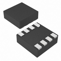
MAX13206EALA+T Maxim Integrated Products, MAX13206EALA+T Datasheet - Page 4

MAX13206EALA+T
Manufacturer Part Number
MAX13206EALA+T
Description
IC ESD PROTECTOR 8-UDFN
Manufacturer
Maxim Integrated Products
Datasheet
1.MAX13208EALBT.pdf
(9 pages)
Specifications of MAX13206EALA+T
Power (watts)
381mW
Polarization
6 Channel Array - Unidirectional
Mounting Type
Surface Mount
Package / Case
8-µDFN
Lead Free Status / RoHS Status
Lead free / RoHS Compliant
Voltage - Breakdown
-
Voltage - Reverse Standoff (typ)
-
2-/4-/6-/8-Channel, ±30kV ESD Protectors in µDFN
The MAX13202E/MAX13204E/MAX13206E/MAX13208E
are diode arrays designed to protect sensitive electron-
ics against damage resulting from ESD conditions or
transient voltages. The low input capacitance makes
these devices ideal for high-speed data lines. The
MAX13202E/MAX13204E/MAX13206E/MAX13208E
protect two, four, six, and eight channels, respectively.
The MAX13202E/MAX13204E/MAX13206E/MAX13208E
are designed to work in conjunction with a device’s
intrinsic ESD protection. The MAX13202E/MAX13204E/
MAX13206E/MAX13208E limit the excursion of the ESD
event to below ±25V peak voltage when subjected to the
Human Body Model waveform. When subjected to the
IEC 61000-4-2 waveform, the peak voltage is limited to
±80V (Contact Discharge) and ±120V (Air-Gap
Discharge). The device that is being protected by the
MAX13202E/MAX13204E/ MAX13206E/MAX13208E
must be able to withstand these peak voltages plus any
additional voltage generated by the parasitic board.
Maximum protection against ESD damage results from
proper board layout (see the Layout Recommendations
section and Figure 2). A good layout reduces the para-
sitic series inductance on the ground line, supply line,
and protected signal lines.
The MAX13202E/MAX13204E/MAX13206E/MAX13208E
ESD diodes clamp the voltage on the protected lines
during an ESD event and shunt the current to GND or
V
defined as the forward voltage drop, V
diode plus any supply voltage present on the cathode.
For positive ESD pulses:
For negative ESD pulses:
In reality, the effect of the parasitic series inductance
on the lines must also be considered (Figure 1).
For positive ESD pulses:
For negative ESD pulses:
4
V
CC
C
_______________________________________________________________________________________
. In an ideal circuit, the clamping voltage, V
=
V
CC
+
V
Applications Information
F D
( )
1
V
+
C
Detailed Description
V
= V
L x
C
1
Design Considerations
= -V
CC
d I
+ V
F
(
ESD
dt
F
)
+
F
, of the protection
L
2
x
d I
(
ESD
dt
C
)
, is
where I
Figure 1. Parasitic Series Inductance
Figure 2. Layout Considerations
V
C
NEGATIVE ESD
CURRENT
PULSE
PATH TO
GROUND
GND
V
PROTECTED LINE
CC
= −
ESD
L1
V
PROTECTED
LINE
is the ESD current pulse.
F D
( )
2
+
L1
POSITIVE SUPPLY RAIL
D1
D2
L x
1
I/O_
d I
L2
L3
GROUND RAIL
I/O_
(
D1
D2
ESD
dt
L2
L3
)
+
V
L
C
3
x
PROTECTED
d I
CIRCUIT
(
ESD
dt
)


