1SMB10CAT3 ON Semiconductor, 1SMB10CAT3 Datasheet
1SMB10CAT3
Specifications of 1SMB10CAT3
Available stocks


Related parts for 1SMB10CAT3

1SMB10CAT3 Summary of contents
Page 1
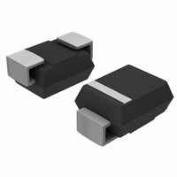
... Series Watt Peak Power Zener Transient Voltage Suppressors Bidirectional* The SMB series is designed to protect voltage sensitive components from high voltage, high energy transients. They have excellent clamping capability, high surge capability, low zener impedance and fast response time. The SMB series is supplied in ON Semiconductor’ ...
Page 2
... Recommended Operating Conditions is not implied. Extended exposure to stresses above the Recommended Operating Conditions may affect device reliability 1000 ms, non−repetitive 2. 1″ square copper pad, FR−4 board 3. FR−4 board, using ON Semiconductor minimum recommended footprint, as shown in 403A case outline dimensions spec *Please see 1SMB5.0AT3 to 1SMB170AT3 for Unidirectional devices ELECTRICAL CHARACTERISTICS (T = 25° ...
Page 3
... ELECTRICAL CHARACTERISTICS V (Note 4) Device Volts Marking Device* 1SMB10CAT3, G KXC 1SMB11CAT3, G KZC 1SMB12CAT3, G LEC 1SMB13CAT3, G LGC 1SMB14CAT3, G LKC 1SMB15CAT3, G LMC 1SMB16CAT3, G LPC 1SMB17CAT3, G LRC 1SMB18CAT3, G LTC 1SMB20CAT3, G LVC 1SMB22CAT3, G LXC 1SMB24CAT3, G LZC 1SMB26CAT3, G MEC 1SMB28CAT3, G MGC 1SMB30CAT3, G MKC 1SMB33CAT3, G MMC 1SMB36CAT3, G MPC ...
Page 4
... Figure 4. Typical Junction Capacitance vs. Bias TYPICAL PROTECTION CIRCUIT Z in LOAD V http://onsemi.com 4 PULSE WIDTH ( DEFINED P AS THAT POINT WHERE THE PEAK CURRENT DECAYS TO 50 HALF VALUE - TIME (ms) Figure 2. Pulse Waveform 1SMB10CAT3G 1SMB18CAT3G 1SMB48CAT3G 1SMB75CAT3G 10 BIAS VOLTAGE (V) Voltage L 5 100 ...
Page 5
RESPONSE TIME In most applications, the transient suppressor device is placed in parallel with the equipment or component to be protected. In this situation, there is a time delay associated with the capacitance of the device and an overshoot condition ...
Page 6
TIME DELAY DUE TO CAPACITIVE EFFECT D Figure 5. 1 0.7 0.5 0.3 0.2 0.1 0.07 0.05 0.03 0.02 0.01 The entire series has Underwriters Laboratory Recognition for the classification of protectors (QVGQ2) ...
Page 7
... H 0.0020 0.0060 0.051 0.152 J 0.006 0.012 0.15 0.30 K 0.030 0.050 0.76 1.27 P 0.020 REF 0.51 REF S 0.205 0.220 5.21 5.59 mm inches ON Semiconductor Website: www.onsemi.com Order Literature: http://www.onsemi.com/orderlit For additional information, please contact your local Sales Representative 1SMB10CAT3/D ...