1SMB5.0AT3G ON Semiconductor, 1SMB5.0AT3G Datasheet - Page 5
1SMB5.0AT3G
Manufacturer Part Number
1SMB5.0AT3G
Description
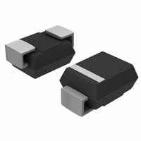
TVS 600W 5.0V UNIDIRECT SMB
Manufacturer
ON Semiconductor
Datasheet
1.1SMB7.0AT3G.pdf
(7 pages)
Specifications of 1SMB5.0AT3G
Voltage - Reverse Standoff (typ)
5V
Voltage - Breakdown
6.4V
Power (watts)
600W
Polarization
Unidirectional
Mounting Type
Surface Mount
Package / Case
DO-214AA, SMB
Number Of Elements
1
Polarity
Uni-Directional
Package Type
SMB
Operating Temperature Classification
Military
Reverse Breakdown Voltage
6.4V
Clamping Voltage
9.2V
Reverse Stand-off Voltage
5V
Leakage Current (max)
800uA
Peak Pulse Current
65.2A
Peak Pulse Power Dissipation
600W
Test Current (it)
10mA
Operating Temp Range
-65C to 150C
Mounting
Surface Mount
Pin Count
2
Operating Voltage
5 V
Breakdown Voltage
6.7 V
Termination Style
SMD/SMT
Peak Surge Current
65.2 A
Maximum Operating Temperature
+ 150 C
Minimum Operating Temperature
- 65 C
Dimensions
3.56 mm W x 4.32 mm L
Lead Free Status / RoHS Status
Lead free / RoHS Compliant
Other names
1SMB5.0AT3GOSTR
Available stocks
Company
Part Number
Manufacturer
Quantity
Price
Company:

Part Number:
1SMB5.0AT3G
Manufacturer:
ON
Quantity:
20 000
Part Number:
1SMB5.0AT3G
Manufacturer:
ON/安森美
Quantity:
20 000


RESPONSE TIME
placed in parallel with the equipment or component to be
protected. In this situation, there is a time delay associated
with the capacitance of the device and an overshoot
condition associated with the inductance of the device and
the inductance of the connection method. The capacitive
effect is of minor importance in the parallel protection
scheme because it only produces a time delay in the
transition from the operating voltage to the clamp voltage as
shown in Figure 6.
turn-on time (time required for the device to go from zero
current to full current) and lead inductance. This inductive
effect produces an overshoot in the voltage across the
equipment or component being protected as shown in
Figure 7. Minimizing this overshoot is very important in the
application, since the main purpose for adding a transient
suppressor is to clamp voltage spikes. The SMB series have
a very good response time, typically < 1.0 ns and negligible
inductance. However, external inductive effects could
produce unacceptable overshoot. Proper circuit layout,
In most applications, the transient suppressor device is
The inductive effects in the device are due to actual
APPLICATION NOTES
http://onsemi.com
5
minimum lead lengths and placing the suppressor device as
close as possible to the equipment or components to be
protected will minimize this overshoot.
prevent overstress of the protection device. This impedance
should be as high as possible, without restricting the circuit
operation.
DUTY CYCLE DERATING
and at a lead temperature of 25°C. If the duty cycle increases,
the peak power must be reduced as indicated by the curves
of Figure 8. Average power must be derated as the lead or
ambient temperature rises above 25°C. The average power
derating curve normally given on data sheets may be
normalized and used for this purpose.
in error as the 10 ms pulse has a higher derating factor than
the 10 ms pulse. However, when the derating factor for a
given pulse of Figure 8 is multiplied by the peak power
value of Figure 1 for the same pulse, the results follow the
expected trend.
Some input impedance represented by Z
The data of Figure 1 applies for non-repetitive conditions
At first glance the derating curves of Figure 8 appear to be
in
is essential to
Related parts for 1SMB5.0AT3G
Image
Part Number
Description
Manufacturer
Datasheet
Request
R

Part Number:
Description:
ON Semiconductor [VOLTAGE REGULATOR]
Manufacturer:
ON Semiconductor
Datasheet:
Part Number:
Description:
357-036-542-201 CARDEDGE 36POS DL .156 BLK LOPRO
Manufacturer:
ON Semiconductor
Datasheet:
Part Number:
Description:
357-036-542-201 CARDEDGE 36POS DL .156 BLK LOPRO
Manufacturer:
ON Semiconductor
Datasheet:
Part Number:
Description:
357-036-542-201 CARDEDGE 36POS DL .156 BLK LOPRO
Manufacturer:
ON Semiconductor
Datasheet:
Part Number:
Description:
357-036-542-201 CARDEDGE 36POS DL .156 BLK LOPRO
Manufacturer:
ON Semiconductor
Datasheet:
Part Number:
Description:
357-036-542-201 CARDEDGE 36POS DL .156 BLK LOPRO
Manufacturer:
ON Semiconductor
Datasheet:
Part Number:
Description:
357-036-542-201 CARDEDGE 36POS DL .156 BLK LOPRO
Manufacturer:
ON Semiconductor
Datasheet:
Part Number:
Description:
357-036-542-201 CARDEDGE 36POS DL .156 BLK LOPRO
Manufacturer:
ON Semiconductor
Datasheet:
Part Number:
Description:
357-036-542-201 CARDEDGE 36POS DL .156 BLK LOPRO
Manufacturer:
ON Semiconductor
Datasheet:
Part Number:
Description:
357-036-542-201 CARDEDGE 36POS DL .156 BLK LOPRO
Manufacturer:
ON Semiconductor
Datasheet:
Part Number:
Description:
357-036-542-201 CARDEDGE 36POS DL .156 BLK LOPRO
Manufacturer:
ON Semiconductor
Datasheet:
Part Number:
Description:
Manufacturer:
ON Semiconductor
Datasheet:
Part Number:
Description:
Manufacturer:
ON Semiconductor
Datasheet:
Part Number:
Description:
Manufacturer:
ON Semiconductor
Datasheet: