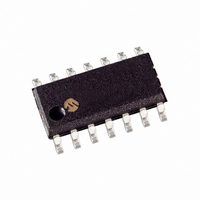
PIC16F688-I/SL Microchip Technology, PIC16F688-I/SL Datasheet - Page 86

PIC16F688-I/SL
Manufacturer Part Number
PIC16F688-I/SL
Description
IC PIC MCU FLASH 4KX14 14SOIC
Manufacturer
Microchip Technology
Series
PIC® 16Fr
Datasheets
1.PIC16F616T-ISL.pdf
(8 pages)
2.PIC16F688T-ISL.pdf
(204 pages)
3.PIC16F688T-ISL.pdf
(6 pages)
4.PIC16F688T-ISL.pdf
(4 pages)
5.PIC16F688T-ISL.pdf
(688 pages)
6.PIC16F688-EP.pdf
(174 pages)
Specifications of PIC16F688-I/SL
Program Memory Type
FLASH
Program Memory Size
7KB (4K x 14)
Package / Case
14-SOIC (3.9mm Width), 14-SOL
Core Processor
PIC
Core Size
8-Bit
Speed
20MHz
Connectivity
UART/USART
Peripherals
Brown-out Detect/Reset, POR, WDT
Number Of I /o
12
Eeprom Size
256 x 8
Ram Size
256 x 8
Voltage - Supply (vcc/vdd)
2 V ~ 5.5 V
Data Converters
A/D 8x10b
Oscillator Type
Internal
Operating Temperature
-40°C ~ 85°C
Processor Series
PIC16F
Core
PIC
Data Bus Width
8 bit
Data Ram Size
256 B
Interface Type
SCI, USART
Maximum Clock Frequency
20 MHz
Number Of Programmable I/os
12
Number Of Timers
1
Operating Supply Voltage
2 V to 5.5 V
Maximum Operating Temperature
+ 85 C
Mounting Style
SMD/SMT
3rd Party Development Tools
52715-96, 52716-328, 52717-734
Development Tools By Supplier
PG164130, DV164035, DV244005, DV164005, PG164120, ICE2000, DM163014, DM164120-4
Minimum Operating Temperature
- 40 C
On-chip Adc
8 bit
Lead Free Status / RoHS Status
Lead free / RoHS Compliant
For Use With
XLT14SO-1 - SOCKET TRANSITION 14SOIC 150/208AC162061 - HEADER INTRFC MPLAB ICD2 20PINAC162056 - HEADER INTERFACE ICD2 16F688
Lead Free Status / Rohs Status
Lead free / RoHS Compliant
Available stocks
Company
Part Number
Manufacturer
Quantity
Price
Company:
Part Number:
PIC16F688-I/SL
Manufacturer:
MICROCHIP
Quantity:
4 952
Company:
Part Number:
PIC16F688-I/SL
Manufacturer:
Microchip Technology
Quantity:
27 564
Part Number:
PIC16F688-I/SL
Manufacturer:
MICROCHIP/微芯
Quantity:
20 000
- PIC16F616T-ISL PDF datasheet
- PIC16F688T-ISL PDF datasheet #2
- PIC16F688T-ISL PDF datasheet #3
- PIC16F688T-ISL PDF datasheet #4
- PIC16F688T-ISL PDF datasheet #5
- PIC16F688-EP PDF datasheet #6
- Current page: 86 of 688
- Download datasheet (3Mb)
PICmicro MID-RANGE MCU FAMILY
5.2
5.3
5.4
DS31005A-page 5-4
General Instruction Format
Central Processing Unit (CPU)
Instruction Clock
The Mid-Range MCU instructions can be broken down into four general formats as shown in
Figure
opcode size is what allows 35 instructions to be implemented.
Figure 5-1: General Format for Instructions
The CPU can be thought of as the “brains” of the device. It is responsible for fetching the correct
instruction for execution, decoding that instruction, and then executing that instruction.
The CPU sometimes works in conjunction with the ALU to complete the execution of the instruc-
tion (in arithmetic and logical operations).
The CPU controls the program memory address bus, the data memory address bus, and
accesses to the stack.
Each instruction cycle (T
as the device oscillator cycle time (T
Decode, Read, Process Data, Write, etc., of each instruction cycle. The following diagram shows
the relationship of the Q cycles to the instruction cycle.
The four Q cycles that make up an instruction cycle (T
Each instruction will show a detailed Q cycle operation for the instruction.
Figure 5-2: Q Cycle Activity
Bit-oriented file register operations
Byte-oriented file register operations
Literal and control operations
General
CALL and GOTO instructions only
Q1:
Q2:
Q3:
Q4:
13
13
13
13
5-1. As can be seen the opcode for the instruction varies from 3-bits to 6-bits. This variable
Tosc
OPCODE
OPCODE
OPCODE
OPCODE
Instruction Decode Cycle or forced No operation
Instruction Read Data Cycle or No operation
Process the Data
Instruction Write Data Cycle or No operation
11
Q1
10 9
10
8
Q2
CY
b (BIT #)
d
T
7
) is comprised of four Q cycles (Q1-Q4). The Q cycle time is the same
8
CY
Q3
1
6
7
7 6
k (literal)
Q4
f (FILE #)
k (literal)
OSC
f (FILE #)
Q1
). The Q cycles provide the timing/designation for the
Q2
0
0
0
0
T
CY
Q3
2
CY
) can be generalized as:
Q4
d = 0 for destination W
d = 1 for destination f
f = 7-bit file register address
b = 3-bit bit address
f = 7-bit file register address
k = 8-bit immediate value
k = 11-bit immediate value
Q1
1997 Microchip Technology Inc.
Q2
T
CY
Q3
3
Q4
Related parts for PIC16F688-I/SL
Image
Part Number
Description
Manufacturer
Datasheet
Request
R

Part Number:
Description:
Manufacturer:
Microchip Technology Inc.
Datasheet:

Part Number:
Description:
IC MCU FLASH 4KX14 14TSSOP
Manufacturer:
Microchip Technology
Datasheet:

Part Number:
Description:
IC PIC MCU FLASH 4KX14 14DIP
Manufacturer:
Microchip Technology
Datasheet:

Part Number:
Description:
IC PIC MCU FLASH 4KX14 16QFN
Manufacturer:
Microchip Technology
Datasheet:

Part Number:
Description:
IC MCU PIC FLASH 4KX14 14SOIC
Manufacturer:
Microchip Technology
Datasheet:

Part Number:
Description:
IC PIC MCU FLASH 4KX14 14TSSOP
Manufacturer:
Microchip Technology
Datasheet:

Part Number:
Description:
IC MCU PIC FLASH 4KX14 14DIP
Manufacturer:
Microchip Technology
Datasheet:

Part Number:
Description:
IC PIC MCU FLASH 4KX14 16QFN
Manufacturer:
Microchip Technology
Datasheet:

Part Number:
Description:
IC PIC MCU FLASH 4KX14 14TSSOP
Manufacturer:
Microchip Technology
Datasheet:

Part Number:
Description:
IC, 8BIT MCU, PIC16F, 32MHZ, SOIC-18
Manufacturer:
Microchip Technology
Datasheet:

Part Number:
Description:
IC, 8BIT MCU, PIC16F, 32MHZ, SSOP-20
Manufacturer:
Microchip Technology
Datasheet:

Part Number:
Description:
IC, 8BIT MCU, PIC16F, 32MHZ, DIP-18
Manufacturer:
Microchip Technology
Datasheet:

Part Number:
Description:
IC, 8BIT MCU, PIC16F, 32MHZ, QFN-28
Manufacturer:
Microchip Technology
Datasheet:

Part Number:
Description:
IC, 8BIT MCU, PIC16F, 32MHZ, QFN-28
Manufacturer:
Microchip Technology
Datasheet:

Part Number:
Description:
IC, 8BIT MCU, PIC16F, 32MHZ, QFN-28
Manufacturer:
Microchip Technology
Datasheet:


