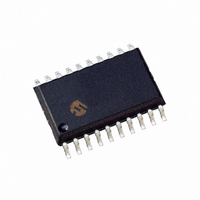
PIC24F04KA201-I/SO Microchip Technology, PIC24F04KA201-I/SO Datasheet - Page 151

PIC24F04KA201-I/SO
Manufacturer Part Number
PIC24F04KA201-I/SO
Description
IC PIC MCU FLASH 512KX4 20-SOIC
Manufacturer
Microchip Technology
Series
PIC® XLP™ 24Fr
Datasheets
1.PIC24F04KA201-ISS.pdf
(8 pages)
2.PIC24F04KA201-ISS.pdf
(48 pages)
3.PIC24F04KA201-ISS.pdf
(224 pages)
4.PIC24F04KA201-ISS.pdf
(26 pages)
Specifications of PIC24F04KA201-I/SO
Core Size
16-Bit
Program Memory Size
4KB (1.375K x 24)
Peripherals
Brown-out Detect/Reset, HLVD, POR, PWM, WDT
Core Processor
PIC
Speed
32MHz
Connectivity
I²C, IrDA, SPI, UART/USART
Number Of I /o
18
Program Memory Type
FLASH
Ram Size
512 x 8
Voltage - Supply (vcc/vdd)
1.8 V ~ 3.6 V
Data Converters
A/D 9x10b
Oscillator Type
Internal
Operating Temperature
-40°C ~ 85°C
Package / Case
20-SOIC (7.5mm Width)
Controller Family/series
PIC24
No. Of I/o's
18
Ram Memory Size
512Byte
Cpu Speed
32MHz
No. Of Timers
3
Processor Series
PIC24F
Core
PIC
Data Bus Width
16 bit
Data Ram Size
512 B
Interface Type
I2C, SPI, UART
Maximum Clock Frequency
32 KHz
Number Of Programmable I/os
12
Number Of Timers
3
Operating Supply Voltage
1.8 V to 3.6 V
Maximum Operating Temperature
+ 125 C
Mounting Style
SMD/SMT
3rd Party Development Tools
52713-733, 52714-737, 53276-922, EWDSPIC
Development Tools By Supplier
PG164130, DV164035, DV244005, DV164005, DM240001
Minimum Operating Temperature
- 40 C
On-chip Adc
10 bit, 9 Channel
Lead Free Status / RoHS Status
Lead free / RoHS Compliant
Eeprom Size
-
Lead Free Status / Rohs Status
Details
- PIC24F04KA201-ISS PDF datasheet
- PIC24F04KA201-ISS PDF datasheet #2
- PIC24F04KA201-ISS PDF datasheet #3
- PIC24F04KA201-ISS PDF datasheet #4
- Current page: 151 of 224
- Download datasheet (4Mb)
REGISTER 19-5:
REGISTER 19-6:
© 2009 Microchip Technology Inc.
bit 15
bit 7
Legend:
R = Readable bit
-n = Value at POR
bit 15-13
bit 12-10
bit 9-6
bit 5-0
bit 15
bit 7
Legend:
R = Readable bit
-n = Value at POR
bit 15-13
bit 12-10
bit 9-6
bit 5-0
U-0
U-0
U-0
U-0
—
—
—
—
Unimplemented: Read as ‘0’
PCFG<12:10>: Analog Input Pin Configuration Control bits
1 = Pin for corresponding analog channel is configured in Digital mode; I/O port read enabled
0 = Pin configured in Analog mode; I/O port read disabled; A/D samples pin voltage
Unimplemented: Read as ‘0’
PCFG<5:0>: Analog Input Pin Configuration Control bits
1 = Pin for corresponding analog channel is configured in Digital mode; I/O port read enabled
0 = Pin configured in Analog mode; I/O port read disabled; A/D samples pin voltage
Unimplemented: Read as ‘0’
CSSL<12:10>: A/D Input Pin Scan Selection bits
1 = Corresponding analog channel selected for input scan
0 = Analog channel omitted from input scan
Unimplemented: Read as ‘0’
CSSL<5:0>: A/D Input Pin Scan Selection bits
1 = Corresponding analog channel selected for input scan
0 = Analog channel omitted from input scan
U-0
U-0
U-0
U-0
—
—
—
—
AD1PCFG: A/D PORT CONFIGURATION REGISTER
AD1CSSL: A/D INPUT SCAN SELECT REGISTER (LOW)
W = Writable bit
‘1’ = Bit is set
W = Writable bit
‘1’ = Bit is set
PCFG5
CSSL5
R/W-0
R/W-0
U-0
U-0
—
—
CSSL12
PCFG12
CSSL4
R/W-0
R/W-0
PCFG4
R/W-0
R/W-0
Preliminary
PIC24F04KA201 FAMILY
U = Unimplemented bit, read as ‘0’
‘0’ = Bit is cleared
U = Unimplemented bit, read as ‘0’
‘0’ = Bit is cleared
CSSL11
CSSL3
R/W-0
R/W-0
PCFG11
PCFG3
R/W-0
R/W-0
CSSL10
CSSL2
R/W-0
R/W-0
PCFG10
PCFG2
R/W-0
R/W-0
x = Bit is unknown
x = Bit is unknown
CSSL1
R/W-0
R/W-0
PCFG1
R/W-0
—
U-0
—
DS39937B-page 149
CSSL0
R/W-0
R/W-0
PCFG0
R/W-0
—
U-0
—
bit 8
bit 0
bit 8
bit 0
Related parts for PIC24F04KA201-I/SO
Image
Part Number
Description
Manufacturer
Datasheet
Request
R

Part Number:
Description:
Manufacturer:
Microchip Technology Inc.
Datasheet:

Part Number:
Description:
Manufacturer:
Microchip Technology Inc.
Datasheet:

Part Number:
Description:
Manufacturer:
Microchip Technology Inc.
Datasheet:

Part Number:
Description:
Manufacturer:
Microchip Technology Inc.
Datasheet:

Part Number:
Description:
Manufacturer:
Microchip Technology Inc.
Datasheet:

Part Number:
Description:
Manufacturer:
Microchip Technology Inc.
Datasheet:

Part Number:
Description:
Manufacturer:
Microchip Technology Inc.
Datasheet:

Part Number:
Description:
Manufacturer:
Microchip Technology Inc.
Datasheet:


