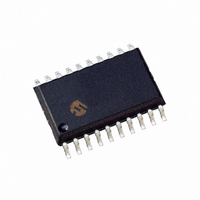
PIC24F04KA201-I/SO Microchip Technology, PIC24F04KA201-I/SO Datasheet - Page 8

PIC24F04KA201-I/SO
Manufacturer Part Number
PIC24F04KA201-I/SO
Description
IC PIC MCU FLASH 512KX4 20-SOIC
Manufacturer
Microchip Technology
Series
PIC® XLP™ 24Fr
Datasheets
1.PIC24F04KA201-ISS.pdf
(8 pages)
2.PIC24F04KA201-ISS.pdf
(48 pages)
3.PIC24F04KA201-ISS.pdf
(224 pages)
4.PIC24F04KA201-ISS.pdf
(26 pages)
Specifications of PIC24F04KA201-I/SO
Core Size
16-Bit
Program Memory Size
4KB (1.375K x 24)
Peripherals
Brown-out Detect/Reset, HLVD, POR, PWM, WDT
Core Processor
PIC
Speed
32MHz
Connectivity
I²C, IrDA, SPI, UART/USART
Number Of I /o
18
Program Memory Type
FLASH
Ram Size
512 x 8
Voltage - Supply (vcc/vdd)
1.8 V ~ 3.6 V
Data Converters
A/D 9x10b
Oscillator Type
Internal
Operating Temperature
-40°C ~ 85°C
Package / Case
20-SOIC (7.5mm Width)
Controller Family/series
PIC24
No. Of I/o's
18
Ram Memory Size
512Byte
Cpu Speed
32MHz
No. Of Timers
3
Processor Series
PIC24F
Core
PIC
Data Bus Width
16 bit
Data Ram Size
512 B
Interface Type
I2C, SPI, UART
Maximum Clock Frequency
32 KHz
Number Of Programmable I/os
12
Number Of Timers
3
Operating Supply Voltage
1.8 V to 3.6 V
Maximum Operating Temperature
+ 125 C
Mounting Style
SMD/SMT
3rd Party Development Tools
52713-733, 52714-737, 53276-922, EWDSPIC
Development Tools By Supplier
PG164130, DV164035, DV244005, DV164005, DM240001
Minimum Operating Temperature
- 40 C
On-chip Adc
10 bit, 9 Channel
Lead Free Status / RoHS Status
Lead free / RoHS Compliant
Eeprom Size
-
Lead Free Status / Rohs Status
Details
program.
PIC24FXXKA2XX
3.4
3.4.1
The NVMCON register controls the Flash memory write
and erase operations. To program the device, set the
NVMCON register to select the type of erase operation
(see
the WR control bit (NVMCON<15>) to initiate the
In ICSP mode, all programming operations are
self-timed. There is an internal delay between setting and
automatic clearing of the WR control bit when the
programming
Section 5.0 “AC/DC Characteristics and Timing
Requirements”
with various programming operations.
3.4.2
The WR bit (NVMCON<15>) is used to start an erase
or write cycle. Initiate the programming cycle by setting
the WR bit.
All erase and write cycles are self-timed. The WR bit
should be polled to determine if the erase or write cycle
is completed. Start a programming cycle as follows:
DS39991A-page 8
BSET
Table
Flash Memory Programming in
ICSP Mode
3-2) or write operation (see
PROGRAMMING OPERATIONS
STARTING AND STOPPING A
PROGRAMMING CYCLE
NVMCON, #WR
operation
for information on the delays associated
is
complete.
Table
Refer
3-3). Set
to
TABLE 3-2:
TABLE 3-3:
4004h
4004h
Note 1:
4064h
404Ch
4068h
405Ah
4059h
4058h
4054h
4058h
Note 1:
NVMCON
NVMCON
Value
Value
(1)
(1)
(1)
(1)
(1)
(1)
The destination address decides the
region (code memory or Configuration
register) of the erased rows/words.
The destination address decides the
region (code memory or Configuration
register) of the erased rows/words.
Write one Configuration register.
Program one row (32 instruction words)
of code memory or executive memory.
Erase the code memory and
Configuration registers (does not erase
programming executive code and
Device ID registers).
Erase the general segment and
Configuration bits associated with it.
Erase the boot segment and
Configuration bits associated with it.
Erase four rows of code memory.
Erase two rows of code memory.
Erase a row of code memory.
Erase all the Configuration registers
(except the code-protect fuses).
Erase Configuration registers except
FBS and FGS.
NVMCON VALUES FOR
ERASE OPERATIONS
NVMCON VALUES FOR
WRITE OPERATIONS
2010 Microchip Technology Inc.
Write Operation
Erase Operation


