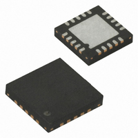
ATTINY2313A-MU Atmel, ATTINY2313A-MU Datasheet - Page 140

ATTINY2313A-MU
Manufacturer Part Number
ATTINY2313A-MU
Description
IC MCU AVR 2K FLASH 20MHZ 20QFN
Manufacturer
Atmel
Series
AVR® ATtinyr
Specifications of ATTINY2313A-MU
Core Processor
AVR
Core Size
8-Bit
Speed
20MHz
Connectivity
I²C, SPI, UART/USART
Peripherals
Brown-out Detect/Reset, POR, PWM, WDT
Number Of I /o
18
Program Memory Size
2KB (1K x 16)
Program Memory Type
FLASH
Eeprom Size
128 x 8
Ram Size
128 x 8
Voltage - Supply (vcc/vdd)
1.8 V ~ 5.5 V
Oscillator Type
Internal
Operating Temperature
-40°C ~ 85°C
Package / Case
20-MLF®, QFN
Processor Series
ATTINY2x
Core
AVR8
Data Bus Width
8 bit
Data Ram Size
128 B
Interface Type
SPI, USART
Maximum Clock Frequency
20 MHz
Number Of Programmable I/os
18
Operating Supply Voltage
1.8 V to 5.5 V
Maximum Operating Temperature
+ 85 C
Mounting Style
SMD/SMT
3rd Party Development Tools
EWAVR, EWAVR-BL
Development Tools By Supplier
ATAVRDRAGON, ATSTK500, ATSTK600, ATAVRISP2, ATAVRONEKIT
Minimum Operating Temperature
- 40 C
Lead Free Status / RoHS Status
Lead free / RoHS Compliant
Data Converters
-
Lead Free Status / Rohs Status
Details
Available stocks
Company
Part Number
Manufacturer
Quantity
Price
Company:
Part Number:
ATTINY2313A-MU
Manufacturer:
ATMEL
Quantity:
313
Company:
Part Number:
ATTINY2313A-MUR
Manufacturer:
LT
Quantity:
4 439
- Current page: 140 of 270
- Download datasheet (7Mb)
14.10.5
140
ATtiny2313A/4313
UBRRL and UBRRH – USART Baud Rate Registers
• Bit 3 – USBS: Stop Bit Select
This bit selects the number of stop bits to be inserted by the Transmitter. The Receiver ignores
this setting.
Table 14-6.
• Bit 2:1 – UCSZ1:0: Character Size
The UCSZ1:0 bits combined with the UCSZ2 bit in UCSRB sets the number of data bits (Char-
acter SiZe) in a frame the Receiver and Transmitter use. See
Table 14-7.
• Bit 0 – UCPOL: Clock Polarity
This bit is used for synchronous mode only. Write this bit to zero when asynchronous mode is
used. The UCPOL bit sets the relationship between data output change and data input sample,
and the synchronous clock (XCK).
Table 14-8.
Bit
0x02 (0x22)
0x09 (0x29)
Bit
Read/Write
Initial Value
UCPOL
0
1
UCSZ2
0
0
0
0
1
1
1
1
Transmitted Data Changed (Output of
TxD Pin)
Rising XCK Edge
Falling XCK Edge
USBS Bit Settings
UCSZ Bits Settings
UCPOL Bit Settings
R/W
15
R
–
7
0
0
USBS
0
1
R/W
14
UCSZ1
R
–
6
0
0
0
0
1
1
0
0
1
1
R/W
13
R
–
5
0
0
R/W
12
Stop Bit(s)
1-bit
2-bit
R
0
–
4
0
UBRR[7:0]
UCSZ0
0
1
0
1
0
1
0
1
R/W
R/W
11
3
0
0
Received Data Sampled (Input on
RxD Pin)
Falling XCK Edge
Rising XCK Edge
R/W
R/W
Character Size
5-bit
6-bit
7-bit
8-bit
Reserved
Reserved
Reserved
9-bit
10
2
0
0
UBRR[11:8]
Table
R/W
R/W
9
1
0
0
14-7.
R/W
R/W
8
0
0
0
UBRRH
UBRRL
8246A–AVR–11/09
Related parts for ATTINY2313A-MU
Image
Part Number
Description
Manufacturer
Datasheet
Request
R

Part Number:
Description:
IC, MCU, 8BIT, 2K FLASH, 20SOIC
Manufacturer:
Atmel
Datasheet:

Part Number:
Description:
IC, MCU, 8BIT, 2K FLASH, 20PDIP
Manufacturer:
Atmel
Datasheet:

Part Number:
Description:
IC, MCU, 8BIT, 8K FLASH, 20PDIP
Manufacturer:
Atmel
Datasheet:

Part Number:
Description:
IC, MCU, 8BIT, 8K FLASH, 20SOIC
Manufacturer:
Atmel
Datasheet:

Part Number:
Description:
DEV KIT FOR AVR/AVR32
Manufacturer:
Atmel
Datasheet:

Part Number:
Description:
INTERVAL AND WIPE/WASH WIPER CONTROL IC WITH DELAY
Manufacturer:
ATMEL Corporation
Datasheet:

Part Number:
Description:
Low-Voltage Voice-Switched IC for Hands-Free Operation
Manufacturer:
ATMEL Corporation
Datasheet:

Part Number:
Description:
MONOLITHIC INTEGRATED FEATUREPHONE CIRCUIT
Manufacturer:
ATMEL Corporation
Datasheet:

Part Number:
Description:
AM-FM Receiver IC U4255BM-M
Manufacturer:
ATMEL Corporation
Datasheet:

Part Number:
Description:
Monolithic Integrated Feature Phone Circuit
Manufacturer:
ATMEL Corporation
Datasheet:

Part Number:
Description:
Multistandard Video-IF and Quasi Parallel Sound Processing
Manufacturer:
ATMEL Corporation
Datasheet:

Part Number:
Description:
High-performance EE PLD
Manufacturer:
ATMEL Corporation
Datasheet:


