PIC18LF13K22-I/P Microchip Technology, PIC18LF13K22-I/P Datasheet - Page 370
PIC18LF13K22-I/P
Manufacturer Part Number
PIC18LF13K22-I/P
Description
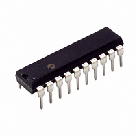
IC PIC MCU FLASH 256KX8 20-PDIP
Manufacturer
Microchip Technology
Series
PIC® XLP™ 18Fr
Datasheets
1.PIC18LF13K22-ISS.pdf
(388 pages)
2.PIC18LF13K22-ISS.pdf
(12 pages)
3.PIC18LF13K22-ISS.pdf
(36 pages)
4.PIC18LF14K22-IP.pdf
(382 pages)
Specifications of PIC18LF13K22-I/P
Program Memory Type
FLASH
Program Memory Size
8KB (4K x 16)
Package / Case
20-DIP (0.300", 7.62mm)
Core Processor
PIC
Core Size
8-Bit
Speed
64MHz
Connectivity
I²C, LIN, SPI, UART/USART
Peripherals
Brown-out Detect/Reset, POR, PWM, WDT
Number Of I /o
17
Eeprom Size
256 x 8
Ram Size
256 x 8
Voltage - Supply (vcc/vdd)
1.8 V ~ 3.6 V
Data Converters
A/D 12x10b
Oscillator Type
Internal
Operating Temperature
-40°C ~ 85°C
Processor Series
PIC18LF
Core
PIC
Data Bus Width
8 bit
Data Ram Size
256 B
Interface Type
I2C, MSSP, SPI, USART
Maximum Clock Frequency
32 KHz
Number Of Programmable I/os
18
Number Of Timers
4
Operating Supply Voltage
1.8 V to 3.6 V
Maximum Operating Temperature
+ 125 C
Mounting Style
Through Hole
3rd Party Development Tools
52715-96, 52716-328, 52717-734, 52712-325, EWPIC18
Development Tools By Supplier
PG164130, DV164035, DV244005, DV164005
Minimum Operating Temperature
- 40 C
On-chip Adc
10 bit, 12 Channel
Lead Free Status / RoHS Status
Lead free / RoHS Compliant
Lead Free Status / RoHS Status
Lead free / RoHS Compliant, Lead free / RoHS Compliant


PIC18F1XK22/LF1XK22
Capture/Compare/PWM (CCP)
CCP1CON Register .......................................................... 113
Clock Accuracy with Asynchronous Operation ................. 184
Clock Sources
CLRF................................................................................. 287
CLRWDT........................................................................... 287
CM1CON0 Register .......................................................... 223
CM2CON0 Register .......................................................... 224
CM2CON1 Register .......................................................... 227
Code Examples
Code Protection ................................................................ 255
COMF................................................................................ 288
Comparator
Comparator Module .......................................................... 217
Comparator Specifications ................................................ 352
Comparator Voltage Reference (CV
Comparators
Compare (CCP Module).................................................... 116
DS41365C-page 370
CCP Pin Configuration .............................................. 115
CCPRxH:CCPRxL Registers .................................... 115
Prescaler ................................................................... 115
Software Interrupt ..................................................... 115
Timer1/Timer3 Mode Selection ................................. 115
Capture Mode. See Capture.
CCP Mode and Timer Resources ............................. 114
Compare Mode. See Compare.
Associated registers.................................................... 26
External Modes
16 x 16 Signed Multiply Routine ................................. 64
16 x 16 Unsigned Multiply Routine ............................. 64
8 x 8 Signed Multiply Routine ..................................... 63
8 x 8 Unsigned Multiply Routine ................................. 63
A/D Conversion ......................................................... 208
Changing Between Capture Prescalers .................... 115
Clearing RAM Using Indirect Addressing.................... 43
Computed GOTO Using an Offset Value .................... 30
Data EEPROM Read .................................................. 61
Data EEPROM Refresh Routine ................................. 62
Data EEPROM Write .................................................. 61
Erasing a Flash Program Memory Row ...................... 55
Fast Register Stack..................................................... 30
Implementing a Timer1 Real-Time Clock.................. 106
Initializing PORTA ....................................................... 80
Initializing PORTB ....................................................... 85
Initializing PORTC....................................................... 90
Loading the SSPBUF (SSPSR) Register .................. 136
Reading a Flash Program Memory Word ................... 54
Saving Status, WREG and BSR Registers in RAM .... 77
Writing to Flash Program Memory ........................ 57–58
Associated Registers ................................................ 228
Operation .................................................................. 217
Operation During Sleep ............................................ 222
Response Time ......................................................... 220
C1 Output State Versus Input Conditions ................. 220
Associated Registers ................................................ 242
Effects of a Reset.............................................. 222, 239
Operation During Sleep ............................................ 239
Response Time ......................................................... 220
Effects of a Reset...................................................... 222
CCPRx Register........................................................ 116
Pin Configuration ...................................................... 116
Software Interrupt ..................................................... 116
HS ....................................................................... 17
LP........................................................................ 17
XT ....................................................................... 17
REF
)
Preliminary
Computed GOTO................................................................ 30
CONFIG1H Register......................................................... 257
CONFIG2H Register......................................................... 259
CONFIG2L Register ......................................................... 258
CONFIG3H Register......................................................... 260
CONFIG4L Register ......................................................... 260
CONFIG5H Register......................................................... 261
CONFIG5L Register ......................................................... 261
CONFIG6H Register......................................................... 262
CONFIG6L Register ......................................................... 262
CONFIG7H Register......................................................... 263
CONFIG7L Register ......................................................... 263
Configuration Bits ............................................................. 256
Configuration Register Protection..................................... 270
Context Saving During Interrupts........................................ 77
CPFSEQ ........................................................................... 288
CPFSGT ........................................................................... 289
CPFSLT ............................................................................ 289
Customer Change Notification Service............................... 11
Customer Notification Service ............................................ 11
Customer Support............................................................... 11
CV
D
Data Addressing Modes ..................................................... 43
Data EEPROM
Data EEPROM Memory...................................................... 59
Data Memory ...................................................................... 33
DAW ................................................................................. 290
DC and AC Characteristics
DC Characteristics
DCFSNZ ........................................................................... 291
DECF ................................................................................ 290
DECFSZ ........................................................................... 291
Development Support ....................................................... 321
Device Differences............................................................ 367
REF
Special Event Trigger ....................................... 112, 116
Timer1/Timer3 Mode Selection................................. 116
Comparing Addressing Modes with the
Direct .......................................................................... 43
Indexed Literal Offset ................................................. 45
Indirect ........................................................................ 43
Inherent and Literal..................................................... 43
Code Protection ........................................................ 270
Associated Registers .................................................. 62
EEADR and EEADRH Registers ................................ 59
EECON1 and EECON2 Registers .............................. 59
Operation During Code-Protect .................................. 62
Protection Against Spurious Write .............................. 62
Reading ...................................................................... 61
Using .......................................................................... 62
Write Verify ................................................................. 61
Writing ........................................................................ 61
Access Bank ............................................................... 37
Access RAM ............................................................... 33
and the Extended Instruction Set ............................... 45
Bank Select Register (BSR) ....................................... 33
General Purpose Registers ........................................ 37
Map for PIC18F13K50/PIC18LF13K50 ...................... 34
Map for PIC18F14K50/PIC18LF14K50 ...................... 35
Special Function Registers ......................................... 37
Graphs and Tables ................................................... 359
Extended and Industrial ............................................ 339
Industrial and Extended ............................................ 329
Voltage Reference Specifications ......................... 352
Extended Instruction Set Enabled ...................... 46
Instructions Affected ........................................... 45
© 2009 Microchip Technology Inc.
Related parts for PIC18LF13K22-I/P
Image
Part Number
Description
Manufacturer
Datasheet
Request
R

Part Number:
Description:
Manufacturer:
Microchip Technology Inc.
Datasheet:
Part Number:
Description:
Manufacturer:
Microchip Technology Inc.
Datasheet:
Part Number:
Description:
Manufacturer:
Microchip Technology Inc.
Datasheet:
Part Number:
Description:
Manufacturer:
Microchip Technology Inc.
Datasheet:
Part Number:
Description:
Manufacturer:
Microchip Technology Inc.
Datasheet:
Part Number:
Description:
Manufacturer:
Microchip Technology Inc.
Datasheet:
Part Number:
Description:
Manufacturer:
Microchip Technology Inc.
Datasheet:
Part Number:
Description:
Manufacturer:
Microchip Technology Inc.
Datasheet: