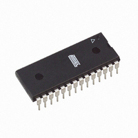
ATMEGA48-20PU Atmel, ATMEGA48-20PU Datasheet - Page 285

ATMEGA48-20PU
Manufacturer Part Number
ATMEGA48-20PU
Description
IC AVR MCU 4K 20MHZ 5V 28DIP
Manufacturer
Atmel
Series
AVR® ATmegar
Datasheets
1.ATAVRTS2080B.pdf
(378 pages)
2.ATMEGA48-20AU.pdf
(35 pages)
3.ATMEGA48-20PU.pdf
(377 pages)
Specifications of ATMEGA48-20PU
Core Processor
AVR
Core Size
8-Bit
Speed
20MHz
Connectivity
I²C, SPI, UART/USART
Peripherals
Brown-out Detect/Reset, POR, PWM, WDT
Number Of I /o
23
Program Memory Size
4KB (2K x 16)
Program Memory Type
FLASH
Eeprom Size
256 x 8
Ram Size
512 x 8
Voltage - Supply (vcc/vdd)
2.7 V ~ 5.5 V
Data Converters
A/D 6x10b
Oscillator Type
Internal
Operating Temperature
-40°C ~ 85°C
Package / Case
28-DIP (0.300", 7.62mm)
Processor Series
ATMEGA48x
Core
AVR8
Data Bus Width
8 bit
Data Ram Size
512 B
Interface Type
2-Wire/SPI/USART/Serial
Maximum Clock Frequency
20 MHz
Number Of Programmable I/os
23
Number Of Timers
3
Operating Supply Voltage
2.7 V to 5.5 V
Maximum Operating Temperature
+ 85 C
Mounting Style
Through Hole
3rd Party Development Tools
EWAVR, EWAVR-BL
Development Tools By Supplier
ATAVRDRAGON, ATSTK500, ATSTK600, ATAVRISP2, ATAVRONEKIT
Minimum Operating Temperature
- 40 C
On-chip Adc
6-ch x 10-bit
Cpu Family
ATmega
Device Core
AVR
Device Core Size
8b
Frequency (max)
20MHz
Total Internal Ram Size
512Byte
# I/os (max)
23
Number Of Timers - General Purpose
3
Operating Supply Voltage (typ)
3.3/5V
Operating Supply Voltage (max)
5.5V
Operating Supply Voltage (min)
2.7V
Instruction Set Architecture
RISC
Operating Temp Range
-40C to 85C
Operating Temperature Classification
Industrial
Mounting
Through Hole
Pin Count
28
Package Type
PDIP
For Use With
ATSTK600-TQFP32 - STK600 SOCKET/ADAPTER 32-TQFPATSTK600 - DEV KIT FOR AVR/AVR32770-1007 - ISP 4PORT ATMEL AVR MCU SPI/JTAGATAVRDRAGON - KIT DRAGON 32KB FLASH MEM AVRATAVRISP2 - PROGRAMMER AVR IN SYSTEMATJTAGICE2 - AVR ON-CHIP D-BUG SYSTEM
Lead Free Status / RoHS Status
Lead free / RoHS Compliant
- Current page: 285 of 378
- Download datasheet (8Mb)
27.2
2545S–AVR–07/10
Fuse Bits
Table 27-3.
Notes:
The ATmega48/88/168 has three Fuse bytes.
tionality of all the fuses and how they are mapped into the Fuse bytes. Note that the fuses are
read as logical zero, “0”, if they are programmed.
Table 27-4.
Extended Fuse Byte
–
–
–
–
–
–
–
SELFPRGEN
BLB0 Mode
BLB1 Mode
1
2
3
4
1
2
3
4
1. Program the Fuse bits and Boot Lock bits before programming the LB1 and LB2.
2. “1” means unprogrammed, “0” means programmed
Lock Bit Protection Modes
Extended Fuse Byte for mega48
BLB02
BLB12
1
1
0
0
1
1
0
0
BLB01
BLB11
Bit No
1
0
0
1
1
0
0
1
7
6
5
4
3
2
1
0
No restrictions for SPM or LPM accessing the Application
section.
SPM is not allowed to write to the Application section.
SPM is not allowed to write to the Application section, and LPM
executing from the Boot Loader section is not allowed to read
from the Application section. If Interrupt Vectors are placed in
the Boot Loader section, interrupts are disabled while executing
from the Application section.
LPM executing from the Boot Loader section is not allowed to
read from the Application section. If Interrupt Vectors are placed
in the Boot Loader section, interrupts are disabled while
executing from the Application section.
No restrictions for SPM or LPM accessing the Boot Loader
section.
SPM is not allowed to write to the Boot Loader section.
SPM is not allowed to write to the Boot Loader section, and LPM
executing from the Application section is not allowed to read
from the Boot Loader section. If Interrupt Vectors are placed in
the Application section, interrupts are disabled while executing
from the Boot Loader section.
LPM executing from the Application section is not allowed to
read from the Boot Loader section. If Interrupt Vectors are
placed in the Application section, interrupts are disabled while
executing from the Boot Loader section.
Description
–
–
–
–
–
–
–
Self Programming Enable
(1)(2)
. Only ATmega88/168.
Table 27-4
-
Table 27-7
ATmega48/88/168
Default Value
1
1
1
1
1
1
1
1 (unprogrammed)
describe briefly the func-
285
Related parts for ATMEGA48-20PU
Image
Part Number
Description
Manufacturer
Datasheet
Request
R

Part Number:
Description:
IC AVR MCU 4K 5V 20MHZ 32-TQFP
Manufacturer:
Atmel
Datasheet:

Part Number:
Description:
Manufacturer:
Atmel Corporation
Datasheet:

Part Number:
Description:
Manufacturer:
Atmel Corporation
Datasheet:

Part Number:
Description:
IC AVR MCU 4K 20MHZ 5V 32TQFP
Manufacturer:
Atmel
Datasheet:

Part Number:
Description:
IC AVR MCU 4K 20MHZ 5V 32-QFN
Manufacturer:
Atmel
Datasheet:

Part Number:
Description:
IC AVR MCU 4K 5V 20MHZ 32-TQFP
Manufacturer:
Atmel
Datasheet:

Part Number:
Description:
IC AVR MCU 4K 5V 20MHZ 32-QFN
Manufacturer:
Atmel
Datasheet:

Part Number:
Description:
IC AVR MCU 4K 5V 20MHZ 32-QFN
Manufacturer:
Atmel
Datasheet:

Part Number:
Description:
IC AVR MCU 4K 5V 20MHZ 28-DIP
Manufacturer:
Atmel
Datasheet:

Part Number:
Description:
IC AVR MCU 4K 5V 20MHZ 28-DIP
Manufacturer:
Atmel
Datasheet:

Part Number:
Description:
IC AVR MCU 4K FLASH 20MHZ 28QFN
Manufacturer:
Atmel
Datasheet:

Part Number:
Description:
MCU AVR 4KB FLASH 20MHZ 32QFN
Manufacturer:
Atmel
Datasheet:


