PIC24F08KA101-I/P Microchip Technology, PIC24F08KA101-I/P Datasheet - Page 4
PIC24F08KA101-I/P
Manufacturer Part Number
PIC24F08KA101-I/P
Description
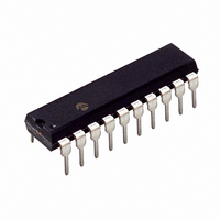
IC PIC MCU FLASH 8K 20-DIP
Manufacturer
Microchip Technology
Series
PIC® XLP™ 24Fr
Datasheets
1.MA240017.pdf
(254 pages)
2.PIC24F04KA201-ISS.pdf
(48 pages)
3.PIC24F16KA101-ISS.pdf
(18 pages)
Specifications of PIC24F08KA101-I/P
Core Size
16-Bit
Program Memory Size
8KB (2.75K x 24)
Core Processor
PIC
Speed
32MHz
Connectivity
I²C, IrDA, SPI, UART/USART
Peripherals
Brown-out Detect/Reset, POR, PWM, WDT
Number Of I /o
18
Program Memory Type
FLASH
Eeprom Size
512 x 8
Ram Size
1.5K x 8
Voltage - Supply (vcc/vdd)
1.8 V ~ 3.6 V
Data Converters
A/D 9x10b
Oscillator Type
Internal
Operating Temperature
-40°C ~ 85°C
Package / Case
20-DIP (0.300", 7.62mm)
Controller Family/series
PIC24
No. Of I/o's
18
Eeprom Memory Size
512Byte
Ram Memory Size
1.5KB
Cpu Speed
32MHz
No. Of Timers
3
Processor Series
PIC24F
Core
PIC
Data Bus Width
16 bit
Data Ram Size
1.5 KB
Interface Type
I2C, IrDA, SPI, UART
Maximum Clock Frequency
32 KHz
Number Of Programmable I/os
18
Number Of Timers
3
Operating Supply Voltage
1.8 V to 3.6 V
Maximum Operating Temperature
+ 125 C
Mounting Style
Through Hole
3rd Party Development Tools
52713-733, 52714-737, 53276-922, EWDSPIC
Development Tools By Supplier
PG164130, DV164035, DV244005, DV164005, DM240001
Minimum Operating Temperature
- 40 C
On-chip Adc
10 bit, 9 Channel
Lead Free Status / RoHS Status
Lead free / RoHS Compliant
For Use With
MA240017 - MODULE PLUG-IN PIC24F16KA102 PIM
Lead Free Status / Rohs Status
Details
Available stocks
Company
Part Number
Manufacturer
Quantity
Price
Company:

Part Number:
PIC24F08KA101-I/P
Manufacturer:
Microchip Technology
Quantity:
135


PIC24F16KA102 FAMILY
5. Module: Memory (Code Protection)
6. Module: Comparator
TABLE 3:
DS80473F-page 4
Param
No.
When any boot segment is enabled in program
memory (FBS<3:1> ≠ 111), it is not possible to
jump directly from the Reset vector to any
address in the boot segment.
Work around
Point the Reset vector to an address in the
general segment. From there, it is possible to
jump into the boot segment.
Affected Silicon Revisions
The maximum value for the input offset voltage
(specification
Table 29-13 of the Device Data Sheet, has
changed for this silicon revision. The new value
is shown in
Work around
None.
Affected Silicon Revisions
A5
A5
X
X
V
Symbol
IOFF
A6
A6
X
Table 3
COMPARATOR DC SPECIFICATIONS (PARTIAL)
A7
A7
Input Offset Voltage
X
D300,
(changes in bold).
B0
B0
X
Characteristics
V
IOFF
),
shown
in
Min
—
Typ
20
7. Module: SPI (Enhanced Buffer Mode)
In Enhanced Buffer mode (SPI1CON2<0> = 1),
polling the SPI Transmit Buffer Full bit, SPITBF
(SPI1STAT<1>), may produce erroneous results.
This occurs only under two circumstances:
a)
b)
For Master mode, this includes all combinations
of the primary prescale bits (SPI11CON1<1:0>)
and secondary prescale bits (SPI1CON1<4:2>)
that, when combined, create an SPI sample
clock divisor with a value of four or greater.
Work around
Instead of polling the SPITBF bit to test for an
empty buffer (SPI1STAT<1> = 0), implement a
SPI receive interrupt handler in software and
add to the SPI transmit buffer in this routine.
Alternatively, poll the SPI Receive Full bit,
SPIRBF (SPI1STAT<0>), or the Shift Register
Empty bit, SRMPT (SPI1STAT<7>), to determine
when to service the SPI transmit and transmit
buffers.
Affected Silicon Revisions
Max
60
A5
X
In Master mode, when the SPI divide clock
is 4 or greater.
In Slave mode, when the SPI sample clock
is slower than 1/4 of the CPU instruction
time (T
A6
Units
X
mV
CY
).
A7
X
2010 Microchip Technology Inc.
B0
Comments
Related parts for PIC24F08KA101-I/P
Image
Part Number
Description
Manufacturer
Datasheet
Request
R

Part Number:
Description:
Manufacturer:
Microchip Technology Inc.
Datasheet:
Part Number:
Description:
Manufacturer:
Microchip Technology Inc.
Datasheet:
Part Number:
Description:
Manufacturer:
Microchip Technology Inc.
Datasheet:
Part Number:
Description:
Manufacturer:
Microchip Technology Inc.
Datasheet:
Part Number:
Description:
Manufacturer:
Microchip Technology Inc.
Datasheet:
Part Number:
Description:
Manufacturer:
Microchip Technology Inc.
Datasheet:
Part Number:
Description:
Manufacturer:
Microchip Technology Inc.
Datasheet:
Part Number:
Description:
Manufacturer:
Microchip Technology Inc.
Datasheet: