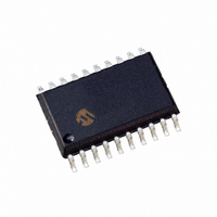
PIC18F14K50-I/SO Microchip Technology, PIC18F14K50-I/SO Datasheet - Page 3

PIC18F14K50-I/SO
Manufacturer Part Number
PIC18F14K50-I/SO
Description
IC PIC MCU FLASH 8KX16 20-SOIC
Manufacturer
Microchip Technology
Series
PIC® XLP™ 18Fr
Datasheets
1.PIC18F13K50-ISS.pdf
(420 pages)
2.PIC18F13K50-ISS.pdf
(10 pages)
3.PIC18F13K50-ISS.pdf
(2 pages)
4.PIC18F14K50-ISS.pdf
(4 pages)
5.PIC18F14K50-IP.pdf
(422 pages)
Specifications of PIC18F14K50-I/SO
Program Memory Type
FLASH
Program Memory Size
16KB (8K x 16)
Package / Case
20-SOIC (7.5mm Width)
Core Processor
PIC
Core Size
8-Bit
Speed
48MHz
Connectivity
I²C, SPI, UART/USART, USB
Peripherals
Brown-out Detect/Reset, POR, PWM, WDT
Number Of I /o
14
Eeprom Size
256 x 8
Ram Size
768 x 8
Voltage - Supply (vcc/vdd)
1.8 V ~ 5.5 V
Data Converters
A/D 11x10b
Oscillator Type
Internal
Operating Temperature
-40°C ~ 85°C
Processor Series
PIC18F
Core
PIC
Data Bus Width
16 bit
Data Ram Size
768 B
Interface Type
EUSART, I2C, MSSP, SPI, USB
Maximum Clock Frequency
48 MHz
Number Of Programmable I/os
15
Number Of Timers
4
Maximum Operating Temperature
+ 85 C
Mounting Style
SMD/SMT
3rd Party Development Tools
52715-96, 52716-328, 52717-734, 52712-325, EWPIC18
Development Tools By Supplier
PG164130, DV164035, DV244005, DV164005
Minimum Operating Temperature
- 40 C
On-chip Adc
10 bit, 11 Channel
Package
20SOIC W
Device Core
PIC
Family Name
PIC18
Maximum Speed
48 MHz
Operating Supply Voltage
3.3|5 V
Lead Free Status / RoHS Status
Lead free / RoHS Compliant
For Use With
AC244023 - PROC EXTENS PAK PIC18F1XK50DV164126 - KIT DEVELOPMENT USB W/PICKIT 2DM164127 - KIT DEVELOPMENT USB 18F14/13K50AC164112 - VOLTAGE LIMITER MPLAB ICD2 VPPXLT20SO1-1 - SOCKET TRANS ICE 20DIP TO 20SOICAC164307 - MODULE SKT FOR PM3 28SSOP
Lead Free Status / Rohs Status
Lead free / RoHS Compliant
Available stocks
Company
Part Number
Manufacturer
Quantity
Price
Company:
Part Number:
PIC18F14K50-I/SO
Manufacturer:
OMRON
Quantity:
1 001
Silicon Errata Issues
1. Module: ADC (Analog-to-Digital
2010 Microchip Technology Inc.
Note:
1.
2.
1.1
Affected Silicon Revisions
1.2
Affected Silicon Revisions
A6
A6
X
X
Select a clock source that is not FRC.
Set the ADIE bit of the PIE1 register and
Work around
clear the ADIF bit of the PIR1 register, then
put the part to Sleep immediately after set-
ting the GO/DONE bit of the ADCON0 reg-
ister.
conversion during Sleep and Wake at the
completion.
including an acquisition time dependent
component (~2 LSb).
The time dependent error is insignificant
the internal FRC oscillator (ADCON2<2:0> =
X11) and the device is not in Sleep, then the
ADC may fail to complete the conversion
which is indicated by the GO/DONE bit of the
ADCON0 register remaining in the GO state
indefinitely. This condition can be cleared by
a device Reset or by clearing the ADON bit
of the ADCON0 register.
Offset error is 3 LSb typical, 7 LSb maximum,
when the time between conversions is less
than 100 ms. When the time since the previ-
ous conversion is greater than 100 ms, take
two ADC conversions and discard the first.
When the ADC is configured to operate with
Work around
This document summarizes all silicon
errata issues from all revisions of silicon,
previous as well as current. Only the
issues indicated by the shaded column in
the following tables apply to the current
silicon revision (A8).
A7
A7
X
Converter)
The
A8
A8
device
will
perform
PIC18F1XK50/PIC18LF1XK50
the
1.3
Affected Silicon Revisions
1.4
Affected Silicon Revisions
1.5
Affected Silicon Revisions
A6
A6
A6
X
X
X
large INL error up to approximately 8 LSb.
Work around
None for the AN3 pin. For better accuracy,
sheet specifications if time between conver-
sions is longer than 10 ms. If the time
between conversions is greater than 10 ms,
the offset error is 1 LSB typical and 3.3 LSB
maximum.
The time dependent error is insignificant
the ADC conversion may not complete prop-
erly. When this occurs, the ADC Interrupt
Flag (ADIF) does not get set, the ADGO/
DONE bit does not get cleared, and the con-
version result does not get loaded into the
ADRESH and ADRESL result registers.
use another analog pin.
Work around
when the time between conversions is less
than 10 ms. When the time between conver-
sions is greater than 10 ms, take two back-
to-back ADC conversions and discard the
results of the first conversion.
Work around
Select the dedicated RC oscillator as the
ADC conversion clock source and perform
all conversions with the device in Sleep.
ADC conversion on AN3/OSC2 will have
The offset error incorrectly exceeds the data
Under certain device operating conditions,
A7
A7
A7
X
X
X
A8
A8
A8
X
DS80411C-page 3


