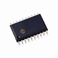
PIC18F14K50-I/SO Microchip Technology, PIC18F14K50-I/SO Datasheet - Page 83

PIC18F14K50-I/SO
Manufacturer Part Number
PIC18F14K50-I/SO
Description
IC PIC MCU FLASH 8KX16 20-SOIC
Manufacturer
Microchip Technology
Series
PIC® XLP™ 18Fr
Datasheets
1.PIC18F13K50-ISS.pdf
(420 pages)
2.PIC18F13K50-ISS.pdf
(10 pages)
3.PIC18F13K50-ISS.pdf
(2 pages)
4.PIC18F14K50-ISS.pdf
(4 pages)
5.PIC18F14K50-IP.pdf
(422 pages)
Specifications of PIC18F14K50-I/SO
Program Memory Type
FLASH
Program Memory Size
16KB (8K x 16)
Package / Case
20-SOIC (7.5mm Width)
Core Processor
PIC
Core Size
8-Bit
Speed
48MHz
Connectivity
I²C, SPI, UART/USART, USB
Peripherals
Brown-out Detect/Reset, POR, PWM, WDT
Number Of I /o
14
Eeprom Size
256 x 8
Ram Size
768 x 8
Voltage - Supply (vcc/vdd)
1.8 V ~ 5.5 V
Data Converters
A/D 11x10b
Oscillator Type
Internal
Operating Temperature
-40°C ~ 85°C
Processor Series
PIC18F
Core
PIC
Data Bus Width
16 bit
Data Ram Size
768 B
Interface Type
EUSART, I2C, MSSP, SPI, USB
Maximum Clock Frequency
48 MHz
Number Of Programmable I/os
15
Number Of Timers
4
Maximum Operating Temperature
+ 85 C
Mounting Style
SMD/SMT
3rd Party Development Tools
52715-96, 52716-328, 52717-734, 52712-325, EWPIC18
Development Tools By Supplier
PG164130, DV164035, DV244005, DV164005
Minimum Operating Temperature
- 40 C
On-chip Adc
10 bit, 11 Channel
Package
20SOIC W
Device Core
PIC
Family Name
PIC18
Maximum Speed
48 MHz
Operating Supply Voltage
3.3|5 V
Lead Free Status / RoHS Status
Lead free / RoHS Compliant
For Use With
AC244023 - PROC EXTENS PAK PIC18F1XK50DV164126 - KIT DEVELOPMENT USB W/PICKIT 2DM164127 - KIT DEVELOPMENT USB 18F14/13K50AC164112 - VOLTAGE LIMITER MPLAB ICD2 VPPXLT20SO1-1 - SOCKET TRANS ICE 20DIP TO 20SOICAC164307 - MODULE SKT FOR PM3 28SSOP
Lead Free Status / Rohs Status
Lead free / RoHS Compliant
Available stocks
Company
Part Number
Manufacturer
Quantity
Price
Company:
Part Number:
PIC18F14K50-I/SO
Manufacturer:
OMRON
Quantity:
1 001
- PIC18F13K50-ISS PDF datasheet
- PIC18F13K50-ISS PDF datasheet #2
- PIC18F13K50-ISS PDF datasheet #3
- PIC18F14K50-ISS PDF datasheet #4
- PIC18F14K50-IP PDF datasheet #5
- Current page: 83 of 420
- Download datasheet (4Mb)
9.0
There are up to three ports available. Some pins of the
I/O ports are multiplexed with an alternate function from
the peripheral features on the device. In general, when
a peripheral is enabled, that pin may not be used as a
general purpose I/O pin.
Each port has three registers for its operation. These
registers are:
• TRIS register (data direction register)
• PORT register (reads the levels on the pins of the
• LAT register (output latch)
The PORTA Data Latch (LATA register) is useful for
read-modify-write operations on the value that the I/O
pins are driving.
A simplified model of a generic I/O port, without the
interfaces to other peripherals, is shown in
FIGURE 9-1:
2010 Microchip Technology Inc.
device)
Note 1:
RD LAT
Data
Bus
WR LAT
or Port
WR TRIS
RD TRIS
RD Port
I/O PORTS
I/O pins have diode protection to V
TRIS Latch
Data Latch
D
D
CK
CK
GENERIC I/O PORT
OPERATION
Q
Q
Q
EN
EN
D
DD
and V
Figure
I/O pin
Buffer
Input
SS
.
9-1.
(1)
Preliminary
9.1
PORTA is 5 bits wide. PORTA<5:4> bits are
bidirectional ports and PORTA<3,1:0> bits are input-
only ports. The corresponding data direction register is
TRISA. Setting a TRISA bit (= 1) will make the
corresponding PORTA pin an input (i.e., disable the
output driver). Clearing a TRISA bit (= 0) will make the
corresponding PORTA pin an output (i.e., enable the
output driver and put the contents of the output latch on
the selected pin).
Reading the PORTA register reads the status of the
pins, whereas writing to it, will write to the PORT latch.
The PORTA Data Latch (LATA) register is also memory
mapped. Read-modify-write operations on the LATA
register read and write the latched output value for
PORTA.
All of the PORTA pins are individually configurable as
interrupt-on-change pins. Control bits in the IOCA
register enable (when set) or disable (when clear) the
interrupt function for each pin.
When set, the RABIE bit of the INTCON register
enables interrupts on all pins which also have their
corresponding IOCA bit set. When clear, the RABIE
bit disables all interrupt-on-changes.
Only pins configured as inputs can cause this interrupt
to occur (i.e., any pin configured as an output is
excluded from the interrupt-on-change comparison).
For enabled interrupt-on-change pins, the values are
compared with the old value latched on the last read of
PORTA. The ‘mismatch’ outputs of the last read are
OR’d together to set the PORTA Change Interrupt flag
bit (RABIF) in the INTCON register.
This interrupt can wake the device from the Sleep
mode, or any of the Idle modes. The user, in the
Interrupt Service Routine, can clear the interrupt in the
following manner:
a)
b)
A mismatch condition will continue to set the RABIF flag
bit. Reading or writing PORTA will end the mismatch
condition and allow the RABIF bit to be cleared. The latch
holding the last read value is not affected by a MCLR nor
Brown-out Reset. After either one of these Resets, the
RABIF flag will continue to be set if a mismatch is present.
Any read or write of PORTA to clear the mis-
match condition (except when PORTA is the
source or destination of a MOVFF instruction).
Clear the flag bit, RABIF.
PORTA, TRISA and LATA Registers
PIC18F/LF1XK50
DS41350E-page 83
Related parts for PIC18F14K50-I/SO
Image
Part Number
Description
Manufacturer
Datasheet
Request
R

Part Number:
Description:
Manufacturer:
Microchip Technology Inc.
Datasheet:

Part Number:
Description:
Manufacturer:
Microchip Technology Inc.
Datasheet:

Part Number:
Description:
Manufacturer:
Microchip Technology Inc.
Datasheet:

Part Number:
Description:
Manufacturer:
Microchip Technology Inc.
Datasheet:

Part Number:
Description:
Manufacturer:
Microchip Technology Inc.
Datasheet:

Part Number:
Description:
Manufacturer:
Microchip Technology Inc.
Datasheet:

Part Number:
Description:
Manufacturer:
Microchip Technology Inc.
Datasheet:

Part Number:
Description:
Manufacturer:
Microchip Technology Inc.
Datasheet:


