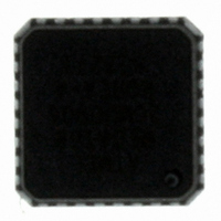
ATMEGA168-20MU Atmel, ATMEGA168-20MU Datasheet - Page 261

ATMEGA168-20MU
Manufacturer Part Number
ATMEGA168-20MU
Description
IC AVR MCU 16K 20MHZ 32-QFN
Manufacturer
Atmel
Series
AVR® ATmegar
Datasheets
1.ATAVRTS2080B.pdf
(378 pages)
2.ATMEGA48-20AU.pdf
(35 pages)
3.ATMEGA88-20MU.pdf
(33 pages)
Specifications of ATMEGA168-20MU
Core Processor
AVR
Core Size
8-Bit
Speed
20MHz
Connectivity
I²C, SPI, UART/USART
Peripherals
Brown-out Detect/Reset, POR, PWM, WDT
Number Of I /o
23
Program Memory Size
16KB (8K x 16)
Program Memory Type
FLASH
Eeprom Size
512 x 8
Ram Size
1K x 8
Voltage - Supply (vcc/vdd)
2.7 V ~ 5.5 V
Data Converters
A/D 8x10b
Oscillator Type
Internal
Operating Temperature
-40°C ~ 85°C
Package / Case
32-VQFN Exposed Pad, 32-HVQFN, 32-SQFN, 32-DHVQFN
Processor Series
ATMEGA16x
Core
AVR8
Data Bus Width
8 bit
Data Ram Size
1 KB
Interface Type
2-Wire, SPI, USART, Serial
Maximum Clock Frequency
20 MHz
Number Of Programmable I/os
23
Number Of Timers
3
Operating Supply Voltage
2.7 V to 5.5 V
Maximum Operating Temperature
+ 85 C
Mounting Style
SMD/SMT
3rd Party Development Tools
EWAVR, EWAVR-BL
Development Tools By Supplier
ATAVRDRAGON, ATSTK500, ATSTK600, ATAVRISP2, ATAVRONEKIT
Minimum Operating Temperature
- 40 C
On-chip Adc
10 bit, 8 Channel
A/d Inputs
8-Channel, 10-Bit
Cpu Speed
20 MIPS
Eeprom Memory
512 Bytes
Input Output
23
Interface
I2C/SPI/UART/USART
Memory Type
Flash
Number Of Bits
8
Package Type
32-pin MLF
Programmable Memory
16K Bytes
Timers
2-8-bit, 1-16-bit
Voltage, Range
4.5-5.5 V
Cpu Family
ATmega
Device Core
AVR
Device Core Size
8b
Frequency (max)
20MHz
Total Internal Ram Size
1KB
# I/os (max)
23
Number Of Timers - General Purpose
3
Operating Supply Voltage (typ)
3.3/5V
Operating Supply Voltage (max)
5.5V
Operating Supply Voltage (min)
2.7V
Instruction Set Architecture
RISC
Operating Temp Range
-40C to 85C
Operating Temperature Classification
Industrial
Mounting
Surface Mount
Pin Count
32
Controller Family/series
AVR MEGA
No. Of I/o's
23
Eeprom Memory Size
512Byte
Ram Memory Size
1KB
No. Of Timers
3
Rohs Compliant
Yes
Package
32MLF EP
Family Name
ATmega
Maximum Speed
20 MHz
For Use With
ATSTK600-TQFP32 - STK600 SOCKET/ADAPTER 32-TQFPATSTK600-DIP40 - STK600 SOCKET/ADAPTER 40-PDIP770-1007 - ISP 4PORT ATMEL AVR MCU SPI/JTAGATAVRDRAGON - KIT DRAGON 32KB FLASH MEM AVRATAVRISP2 - PROGRAMMER AVR IN SYSTEMATJTAGICE2 - AVR ON-CHIP D-BUG SYSTEM
Lead Free Status / RoHS Status
Lead free / RoHS Compliant
Available stocks
Company
Part Number
Manufacturer
Quantity
Price
- Current page: 261 of 378
- Download datasheet (8Mb)
25. Self-Programming the Flash, ATmega48
25.1
25.1.1
25.1.2
2545S–AVR–07/10
Overview
Performing Page Erase by SPM
Filling the Temporary Buffer (Page Loading)
In ATmega48, there is no Read-While-Write support, and no separate Boot Loader Section. The
SPM instruction can be executed from the entire Flash.
The device provides a Self-Programming mechanism for downloading and uploading program
code by the MCU itself. The Self-Programming can use any available data interface and associ-
ated protocol to read code and write (program) that code into the Program memory.
The Program memory is updated in a page by page fashion. Before programming a page with
the data stored in the temporary page buffer, the page must be erased. The temporary page buf-
fer is filled one word at a time using SPM and the buffer can be filled either before the Page
Erase command or between a Page Erase and a Page Write operation:
Alternative 1, fill the buffer before a Page Erase
• Fill temporary page buffer
• Perform a Page Erase
• Perform a Page Write
Alternative 2, fill the buffer after Page Erase
• Perform a Page Erase
• Fill temporary page buffer
• Perform a Page Write
If only a part of the page needs to be changed, the rest of the page must be stored (for example
in the temporary page buffer) before the erase, and then be re-written. When using alternative 1,
the Boot Loader provides an effective Read-Modify-Write feature which allows the user software
to first read the page, do the necessary changes, and then write back the modified data. If alter-
native 2 is used, it is not possible to read the old data while loading since the page is already
erased. The temporary page buffer can be accessed in a random sequence. It is essential that
the page address used in both the Page Erase and Page Write operation is addressing the same
page.
To execute Page Erase, set up the address in the Z-pointer, write “00000011” to SPMCSR and
execute SPM within four clock cycles after writing SPMCSR. The data in R1 and R0 is ignored.
The page address must be written to PCPAGE in the Z-register. Other bits in the Z-pointer will
be ignored during this operation.
• The CPU is halted during the Page Erase operation.
To write an instruction word, set up the address in the Z-pointer and data in R1:R0, write
“00000001” to SPMCSR and execute SPM within four clock cycles after writing SPMCSR. The
content of PCWORD in the Z-register is used to address the data in the temporary buffer. The
temporary buffer will auto-erase after a Page Write operation or by writing the RWWSRE bit in
SPMCSR. It is also erased after a system reset. Note that it is not possible to write more than
one time to each address without erasing the temporary buffer.
ATmega48/88/168
261
Related parts for ATMEGA168-20MU
Image
Part Number
Description
Manufacturer
Datasheet
Request
R

Part Number:
Description:
Manufacturer:
Atmel Corporation
Datasheet:

Part Number:
Description:
Manufacturer:
Atmel Corporation
Datasheet:

Part Number:
Description:
Manufacturer:
ATMEL Corporation
Datasheet:

Part Number:
Description:
IC AVR MCU 16K 20MHZ 32TQFP
Manufacturer:
Atmel
Datasheet:

Part Number:
Description:
IC AVR MCU 16K 20MHZ 28DIP
Manufacturer:
Atmel
Datasheet:

Part Number:
Description:
MCU AVR 16K FLASH 15MHZ 32-TQFP
Manufacturer:
Atmel
Datasheet:

Part Number:
Description:
MCU AVR 16K FLASH 15MHZ 32-QFN
Manufacturer:
Atmel
Datasheet:

Part Number:
Description:
IC AVR MCU 16K 20MHZ 32TQFP
Manufacturer:
Atmel
Datasheet:

Part Number:
Description:
MCU AVR 16KB FLASH 20MHZ 32QFN
Manufacturer:
Atmel
Datasheet:

Part Number:
Description:
MCU AVR 16KB FLASH 20MHZ 32TQFP
Manufacturer:
Atmel
Datasheet:

Part Number:
Description:
IC MCU AVR 16K FLASH 32-QFN
Manufacturer:
Atmel
Datasheet:


