PIC32MX420F032H-40I/MR Microchip Technology, PIC32MX420F032H-40I/MR Datasheet - Page 51
PIC32MX420F032H-40I/MR
Manufacturer Part Number
PIC32MX420F032H-40I/MR
Description
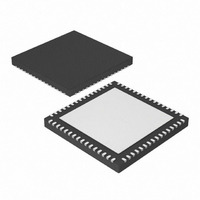
IC PIC MCU FLASH 32KX32 64-QFN
Manufacturer
Microchip Technology
Series
PIC® 32MXr
Datasheets
1.MA320002.pdf
(208 pages)
2.DM320001.pdf
(44 pages)
3.PIC32MX320F032H-40IPT.pdf
(48 pages)
4.PIC32MX320F032H-40IPT.pdf
(66 pages)
5.PIC32MX320F032H-40IPT.pdf
(22 pages)
6.PIC32MX320F064H-40IMR.pdf
(172 pages)
Specifications of PIC32MX420F032H-40I/MR
Core Size
32-Bit
Program Memory Size
32KB (32K x 8)
Core Processor
MIPS32® M4K™
Speed
40MHz
Connectivity
I²C, IrDA, LIN, PMP, SPI, UART/USART, USB OTG
Peripherals
Brown-out Detect/Reset, DMA, POR, PWM, WDT
Number Of I /o
53
Program Memory Type
FLASH
Ram Size
8K x 8
Voltage - Supply (vcc/vdd)
2.3 V ~ 3.6 V
Data Converters
A/D 16x10b
Oscillator Type
Internal
Operating Temperature
-40°C ~ 85°C
Package / Case
64-VFQFN, Exposed Pad
Controller Family/series
PIC32
Ram Memory Size
8KB
Cpu Speed
40MHz
No. Of Timers
5
Interface
EUSART, I2C, SPI, USB
No. Of Pwm Channels
5
Embedded Interface Type
EUSART, I2C, SPI, USB
Rohs Compliant
Yes
Processor Series
PIC32MX4xx
Core
MIPS
Data Bus Width
32 bit
Data Ram Size
8 KB
Interface Type
I2C, JTAG, SPI, TWI, UART, USB
Maximum Clock Frequency
80 MHz
Number Of Programmable I/os
51
Number Of Timers
5
Operating Supply Voltage
2.3 V to 3.6 V
Maximum Operating Temperature
+ 125 C
Mounting Style
SMD/SMT
3rd Party Development Tools
52713-733, 52714-737
Development Tools By Supplier
PG164130, DV164035, DV244005, DV164005, DM320003, DM320002, MA320002
Minimum Operating Temperature
- 40 C
On-chip Adc
10 bit
Lead Free Status / RoHS Status
Lead free / RoHS Compliant
For Use With
876-1000 - PIC32 BREAKOUT BOARD
Eeprom Size
-
Lead Free Status / Rohs Status
Details


TABLE 4-18:
TABLE 4-19:
TABLE 4-20:
BF88_61D0
Legend:
Note
Legend:
Note
Legend:
BF88_61E0
BF80_7000
BF80_7010 PMMODE
BF80_7020
BF80_7030
BF80_7040
BF80_7050
BF80_7060
BF80_F200 DDPCON
Virtual
Virtual
Virtual
Addr
Addr
Addr
SFR
SFR
SFR
1:
2:
1:
PMADDR
PMDOUT
PMSTAT
x = unknown value on Reset, — = unimplemented, read as ‘0’. Reset values are shown in hexadecimal.
CNEN and CNPUE bit(s) are not implemented on 64-pin devices, and read as ‘0’.
All registers in this table have corresponding CLR, SET, and INV Registers at their virtual addresses, plus offsets of 0x4, 0x8, and 0xC, respectively. See Section 12.1.1 “CLR, SET and INV Registers” for more infor-
mation.
PMCON
x = unknown value on Reset, — = unimplemented, read as ‘0’. Reset values are shown in hexadecimal.
All registers in this table have corresponding CLR, SET, and INV Registers at their virtual addresses, plus offsets of 0x4, 0x8, and 0xC, respectively. See Section 12.1.1 “CLR, SET and INV Registers” for more infor-
mation.
x = unknown value on Reset, — = unimplemented, read as ‘0’. Reset values are shown in hexadecimal.
CNPUE
PMAEN
PMDIN
Name
Name
Name
CNEN
SFR
SFR
SFR
CHANGE NOTICE AND PULL-UP REGISTERS MAP
PARALLEL MASTER PORT REGISTERS MAP
PROGRAMMING AND DIAGNOSTICS REGISTERS MAP
31:16
31:16
31:16
31:16
31:16
31:16
31:16
31:16
31:16
31:16
15:0
15:0
15:0
15:0
15:0 CS2EN/A15 CS1EN/A14
15:0
15:0
15:0
15:0
15:0
31/15
31/15
31/15
BUSY
Bits
Bits
Bits
IBF
ON
—
—
—
—
—
—
—
—
—
30/14
30/14
30/14
IBOV
Bits
Bits
Bits
FRZ
—
—
—
—
—
—
—
—
—
IRQM<1:0>
29/13
29/13
29/13
Bits
SIDL
Bits
Bits
—
—
—
—
—
—
—
—
—
—
28/12
Bits
28/12
28/12
Bits
Bits
—
—
ADRMUX<1:0>
—
—
—
—
—
—
—
—
INCM<1:0>
27/11
Bits
27/11
27/11
IB3F
—
—
Bits
Bits
—
—
—
—
—
—
—
MODE16
26/10
PMPTTL
Bits
26/10
26/10
—
—
IB2F
Bits
Bits
—
—
—
—
—
—
—
(1)
PTWREN
Bits
25/9
(2)
—
—
25/9
25/9
IB1F
Bits
Bits
—
—
—
—
—
—
—
MODE<1:0>
(CONTINUED)
PTRDEN
Bits
24/8
—
—
DATAOUT<31:0>
Bits
24/8
Bits
24/8
IB0F
CNPUE<15:0>
DATAIN<31:0>
—
—
—
—
—
—
—
CNEN<15:0>
PTEN<15:0>
DDPUSB
23/7
Bits
—
Bits
23/7
Bits
23/7
OBE
—
—
—
—
—
—
—
ADDR<13:0>
WAITB<1:0>
CSF<1:0>
DDPU1
Bits
22/6
—
OBUF
Bits
22/6
Bits
22/6
—
—
—
—
—
—
—
DDPU2
CNPUE21
CNEN21
Bits
21/5
—
Bits
21/5
Bits
21/5
ALP
—
—
—
—
—
—
(1)
(1)
DDPSPI1
20/4
CNPUE20
Bits
CNEN20
—
CS2P
20/4
20/4
Bits
Bits
—
—
—
—
—
—
WAITM<3:0>
(1)
(1)
JTAGEN
Bits
19/3
CNPUE19
CNEN19
—
CS1P
OB3E
19/3
19/3
Bits
Bits
—
—
—
—
—
(1)
(1)
TROEN
Bits
18/2
—
CNPUE18 CNPUE17 CNPUE16
CNEN18
OB2E
18/2
18/2
Bits
Bits
—
—
—
—
—
—
17/1
Bits
—
—
CNEN17
WRSP
OB1E
Bits
17/1
Bits
17/1
—
—
—
—
—
WAITE<1:0>
16/0
Bits
—
—
CNEN16
RDSP
OB0E
Bits
16/0
Bits
16/0
—
—
—
—
—
Related parts for PIC32MX420F032H-40I/MR
Image
Part Number
Description
Manufacturer
Datasheet
Request
R

Part Number:
Description:
Manufacturer:
Microchip Technology Inc.
Datasheet:
Part Number:
Description:
Manufacturer:
Microchip Technology Inc.
Datasheet:
Part Number:
Description:
Manufacturer:
Microchip Technology Inc.
Datasheet:
Part Number:
Description:
Manufacturer:
Microchip Technology Inc.
Datasheet:
Part Number:
Description:
Manufacturer:
Microchip Technology Inc.
Datasheet:
Part Number:
Description:
Manufacturer:
Microchip Technology Inc.
Datasheet:
Part Number:
Description:
Manufacturer:
Microchip Technology Inc.
Datasheet:
Part Number:
Description:
Manufacturer:
Microchip Technology Inc.
Datasheet: