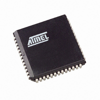
AT89C5130A-S3SUM Atmel, AT89C5130A-S3SUM Datasheet - Page 15

AT89C5130A-S3SUM
Manufacturer Part Number
AT89C5130A-S3SUM
Description
IC 8051 MCU FLASH 16K USB 52PLCC
Manufacturer
Atmel
Series
AT89C513xr
Datasheet
1.AT89C5130A-PUTUM.pdf
(188 pages)
Specifications of AT89C5130A-S3SUM
Core Processor
C52X2
Core Size
8-Bit
Speed
48MHz
Connectivity
I²C, SPI, UART/USART, USB
Peripherals
LED, POR, PWM, WDT
Number Of I /o
34
Program Memory Size
16KB (16K x 8)
Program Memory Type
FLASH
Eeprom Size
4K x 8
Ram Size
1.25K x 8
Voltage - Supply (vcc/vdd)
2.7 V ~ 5.5 V
Oscillator Type
Internal
Operating Temperature
-40°C ~ 85°C
Package / Case
52-PLCC
Processor Series
AT89x
Core
8051
Data Bus Width
8 bit
Data Ram Size
1.25 KB
Interface Type
2-Wire, EUART, SPI, USB
Maximum Clock Frequency
48 MHz
Number Of Programmable I/os
34
Number Of Timers
16 bit
Operating Supply Voltage
2.7 V to 5.5 V
Maximum Operating Temperature
+ 85 C
Mounting Style
SMD/SMT
3rd Party Development Tools
PK51, CA51, A51, ULINK2
Development Tools By Supplier
AT89STK-05
Minimum Operating Temperature
- 40 C
For Use With
AT89OCD-01 - USB EMULATOR FOR AT8XC51 MCU
Lead Free Status / RoHS Status
Lead free / RoHS Compliant
Data Converters
-
Lead Free Status / Rohs Status
Details
Other names
AT89C5130A-S3SIM
AT89C5130A-S3SIM
AT89C5130A-S3SIM
Available stocks
Company
Part Number
Manufacturer
Quantity
Price
- Current page: 15 of 188
- Download datasheet (2Mb)
5.3
5.3.1
Figure 5-3.
4337K–USB–04/08
PLL
PLL Description
CLOCK
OSC
PLL Block Diagram and Symbol
N divider
In order to optimize the power consumption, the oscillator inverter is inactive when the PLL out-
put is not selected for the USB device.
Figure 5-2.
The AT89C5130A/31A-M PLL is used to generate internal high frequency clock (the USB Clock)
synchronized with an external low-frequency (the Peripheral Clock). The PLL clock is used to
generate the USB interface clock. Figure 5-3 shows the internal structure of the PLL.
The PFLD block is the Phase Frequency Comparator and Lock Detector. This block makes the
comparison between the reference clock coming from the N divider and the reverse clock com-
ing from the R divider and generates some pulses on the Up or Down signal depending on the
edge position of the reverse clock. The PLLEN bit in PLLCON register is used to enable the
clock generation. When the PLL is locked, the bit PLOCK in PLLCON register (see Figure 5-3) is
set.
The CHP block is the Charge Pump that generates the voltage reference for the VCO by inject-
ing or extracting charges from the external filter connected on PLLF pin (see Figure 5-4). Value
of the filter components are detailed in the Section “DC Characteristics”.
The VCO block is the Voltage Controlled Oscillator controlled by the voltage V
the charge pump. It generates a square wave signal: the PLL clock.
N3:0
Crystal Connection
PLLCON.1
PLLCON.0
PLOCK
PLLEN
USBclk
PFLD
Down
=
Up
OSCclk
---------------------------------------------- -
R divider
VSS
R3:0
PLLF
CHP
N
+
×
1
(
C1
C2
R
+
Vref
1
)
Q
VCO
X1
X2
AT89C5130A/31A-M
USB Clock Symbol
USB Clock
CLOCK
USB
REF
produced by
15
Related parts for AT89C5130A-S3SUM
Image
Part Number
Description
Manufacturer
Datasheet
Request
R

Part Number:
Description:
Manufacturer:
Atmel Corporation
Datasheet:

Part Number:
Description:
IC 8051 MCU FLASH 16K USB 32QFN
Manufacturer:
Atmel
Datasheet:

Part Number:
Description:
IC 8051 MCU FLASH 16K USB 64VQFP
Manufacturer:
Atmel
Datasheet:

Part Number:
Description:
MCU 8051 16K FLASH USB 64-VQFP
Manufacturer:
Atmel
Datasheet:

Part Number:
Description:
IC 8051 MCU FLASH 16K USB 64VQFP
Manufacturer:
Atmel
Datasheet:

Part Number:
Description:
8-bit Microcontrollers - MCU Microcontroller
Manufacturer:
Atmel

Part Number:
Description:
IC MICRO CTRL 24MHZ 44TQFP
Manufacturer:
Atmel
Datasheet:

Part Number:
Description:
IC MICRO CTRL 24MHZ 44PLCC
Manufacturer:
Atmel
Datasheet:

Part Number:
Description:
IC MICRO CTRL 24MHZ 44PLCC
Manufacturer:
Atmel
Datasheet:

Part Number:
Description:
IC MICRO CTRL 24MHZ 40DIP
Manufacturer:
Atmel
Datasheet:

Part Number:
Description:
IC MICRO CTRL 24MHZ 40DIP
Manufacturer:
Atmel
Datasheet:

Part Number:
Description:
8-bit microcontroller with 4K bytes flash, 5V, 20MHz
Manufacturer:
ATMEL Corporation
Datasheet:

Part Number:
Description:
8-bit microcontroller with 4K bytes flash, 5V, 20MHz
Manufacturer:
ATMEL Corporation
Datasheet:


