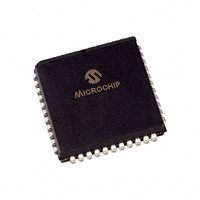
PIC18F442-I/L Microchip Technology, PIC18F442-I/L Datasheet - Page 16

PIC18F442-I/L
Manufacturer Part Number
PIC18F442-I/L
Description
IC MCU FLASH 8KX16 EE A/D 44PLCC
Manufacturer
Microchip Technology
Series
PIC® 18Fr
Datasheets
1.PIC16F616T-ISL.pdf
(8 pages)
2.PIC18F242-ISO.pdf
(332 pages)
3.PIC18F242-ISO.pdf
(14 pages)
4.PIC18F242-ISO.pdf
(16 pages)
5.PIC18F242-ISO.pdf
(16 pages)
6.PIC18F242-ISO.pdf
(14 pages)
7.PIC18LF242-ISO.pdf
(36 pages)
Specifications of PIC18F442-I/L
Core Size
8-Bit
Program Memory Size
16KB (8K x 16)
Core Processor
PIC
Speed
40MHz
Connectivity
I²C, SPI, UART/USART
Peripherals
Brown-out Detect/Reset, LVD, POR, PWM, WDT
Number Of I /o
34
Program Memory Type
FLASH
Eeprom Size
256 x 8
Ram Size
768 x 8
Voltage - Supply (vcc/vdd)
4.2 V ~ 5.5 V
Data Converters
A/D 8x10b
Oscillator Type
External
Operating Temperature
-40°C ~ 85°C
Package / Case
44-PLCC
Controller Family/series
PIC18
No. Of I/o's
34
Eeprom Memory Size
256Byte
Ram Memory Size
768Byte
Cpu Speed
40MHz
No. Of Timers
4
Processor Series
PIC18F
Core
PIC
Data Bus Width
8 bit
Data Ram Size
768 B
Interface Type
MSSP, SPI, I2C, PSP, USART
Maximum Clock Frequency
40 MHz
Number Of Programmable I/os
34
Number Of Timers
1 x 16 bit
Operating Supply Voltage
2 V to 5.5 V
Maximum Operating Temperature
+ 85 C
Mounting Style
SMD/SMT
3rd Party Development Tools
52715-96, 52716-328, 52717-734, 52712-325, EWPIC18
Development Tools By Supplier
PG164130, DV164035, DV244005, DV164005, PG164120, ICE2000, ICE4000, DM163022, DV164136
Minimum Operating Temperature
- 40 C
On-chip Adc
8
Package
44PLCC
Device Core
PIC
Family Name
PIC18
Maximum Speed
40 MHz
Lead Free Status / RoHS Status
Lead free / RoHS Compliant
For Use With
AC164309 - MODULE SKT FOR PM3 44PLCCXLT44L2 - SOCKET TRAN ICE 44PLCC444-1001 - DEMO BOARD FOR PICMICRO MCUDVA16XL441 - ADAPTER DEVICE ICE 44PLCCDV007003 - PROGRAMMER UNIVERSAL PROMATE II
Lead Free Status / Rohs Status
Details
Other names
PIC18F442I/L
Available stocks
Company
Part Number
Manufacturer
Quantity
Price
Company:
Part Number:
PIC18F442-I/L
Manufacturer:
Microchip Technology
Quantity:
10 000
PIC18FXX2/XX8
3.3
Data EEPROM is accessed one byte at a time via an
Address Pointer, EEADR, and a data latch, EEDATA.
Data EEPROM is written by loading EEADR with the
desired memory location, EEDATA with the data to be
written, and initiating a memory write by appropriately
configuring the EECON1 and EECON2 registers. A
byte write automatically erases the location and writes
the new data (erase-before-write).
When using the EECON1 register to perform a data
EEPROM write, the EEPGD bit must be cleared
(EECON1<7> = 0) and the CFGS bit must be cleared
(EECON1<6> = 0). The WREN bit must be set
(EECON1<2> = 1) to enable writes of any sort, and this
must be done prior to initiating a write sequence. The
write sequence is initiated by the setting the WR bit
(EECON1<1> = 1). It is strongly recommended that the
WREN bit be set only when absolutely necessary.
To help prevent inadvertent writes when using the
EECON1 register, EECON2 is used to “enable” the WR
bit. This register must be sequentially loaded with 55h
and then, AAh, immediately prior to asserting the WR
bit in order for the write to occur.
The write will begin on the falling edge of the 4th SCLK
after the WR bit is set.
After the programming sequence terminates, SCLK
must still be held low for the time specified by
parameter P10 to allow high voltage discharge of the
memory array.
FIGURE 3-8:
DS39576C-page 16
SCLK
SDATA
Poll WR bit
Data EEPROM Programming
4-bit Command
1
0
2
0
3
0
SDATA
SCLK
4
0
DATA EEPROM WRITE TIMING
P5
BSF EECON1, WR
1
4-bit Command
1
0
2
2
0
15 16
3
0
4
0
P5A
P5
MOVF EECON1, W, 0
1
2
SDATA = Input
SDATA = Input
15 16
P5A
4-bit Command
1
0
Poll WR bit, Repeat Until Clear
FIGURE 3-7:
2
0
3
0
(see below)
4
0
P5
MOVWF TABLAT
1
No
2
Unlock Sequence
15 16
AAh - EECON2
55h - EECON2
PROGRAM DATA FLOW
Enable Write
Set Address
Start Write
Sequence
2010 Microchip Technology Inc.
Set Data
WR bit
Done?
clear?
Start
Done
P5A
Yes
Yes
(see Figure 4-6)
SDATA = Output
Shift Out Data
No
P10
16-bit Data
Payload
1
n
2
n


