AT91SAM7A3-AU Atmel, AT91SAM7A3-AU Datasheet
AT91SAM7A3-AU
Specifications of AT91SAM7A3-AU
Available stocks


Related parts for AT91SAM7A3-AU


AT91SAM7A3-AU Summary of contents
Page 1
... One USB 2.0 Full Speed (12 Mbits per Second) Device Port – On-chip Transceiver, 2376-byte Configurable Integrated FIFOs ® ® Thumb Processor Product Description AT91SAM7A3 Preliminary Summary NOTE: This is a summary document. The complete document is available on the Atmel website at www.atmel.com. 6042DS–ATARM–14-Dec-06 ...
Page 2
... VDD1V8 Output of the Voltage Regulator and Core Power Supply – 3.6V VDDANA ADC Power Supply – 3.6V VDDBU Backup Power Supply • 5V-tolerant I/Os • Fully Static Operation MHz at 1.65V and 85°C Worst Case Conditions • Available in a 100-lead LQFP Green Package AT91SAM7A3 2 ® Infrared Modulation/Demodulation 6042DS–ATARM–14-Dec-06 ...
Page 3
... By combining a high-performance 32-bit RISC processor with a high-density 16-bit instruction set, Flash and SRAM memory, a wide range of peripherals including CAN controllers, 10-bit ADC, Timers and serial communication channels monolithic chip, the AT91SAM7A3 is ideal for many compute-intensive embedded control applications. 6042DS–ATARM–14-Dec-06 AT91SAM7A3 ™ ...
Page 4
... Block Diagram Figure 2-1. AT91SAM7A3 Block Diagram TDI TDO TMS TCK JTAGSEL System Controller TST FIQ IRQ0-IRQ3 DRXD DTXD PCK0-PCK3 PLLRC PLL XIN OSC XOUT GND VDDBU RCOSC FWKUP WKUP0 WKUP1 SHDW POR VDDBU VDD3V3 POR VDD1V8 POR NRST PIOA RXD0 ...
Page 5
... ICE and JTAG Input Input Output Input Input Reset/Test I/O Input Debug Unit Input Output AT91SAM7A3 Level Comments 3. 3.6V 1.85V typical 1.65V to 1.95V Open Drain. Accept between 0V and VDDBU Accept between 0V and VDDBU External pull-up resistor needed. No pull-up resistor ...
Page 6
... TF0 - TF1 Transmit Frame Sync RF0 - RF1 Receive Frame Sync TCLK0 - TCLK8 External Clock Input TIOA0 - TIOA8 I/O Line A TIOB0 - TIOB8 I/O Line B PWM0 - PWM7 PWM Channels AT91SAM7A3 6 Active Type AIC Input Input PIO I/O I/O Multimedia Card Interface Output I/O ...
Page 7
... ADC Trigger ADC1_ADTRG CANRX0-CANRX1 CAN Inputs CANTX0-CANTX1 CAN Outputs 6042DS–ATARM–14-Dec-06 Active Type Level SPI I/O I/O I/O I/O Output Two-wire Interface I/O I/O Analog-to-Digital Converter Analog Analog Input CAN Controller Input Output AT91SAM7A3 Comments Low Low Digital pulled-up inputs at reset 7 ...
Page 8
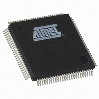
... Package 4.1 100-lead LQFP Package Outline Figure 4-1 tion is given in the Mechanical Characteristics section of the full datasheet. Figure 4-1. AT91SAM7A3 8 shows the orientation of the 100-lead LQFP package. A detailed mechanical descrip- 100-lead LQFP Outline (Top View 100 6042DS–ATARM–14-Dec-06 ...
Page 9
... PA8 61 VDD3V3 PA9 62 VDD3V3 63 GND 64 VDD1V8 65 PA10 66 JTAGSEL PA11 67 PA12 68 PA13 69 PA14 70 PA15 71 PA16 72 VDDPLL PA17 73 PA18 74 PA19 75 AT91SAM7A3 PA20 76 PLLRC PA21 77 VDDANA PA22 78 ADVREFP PA23 79 GND PA24 80 PB14/ADC0_AD0 PA25 81 PB15/ADC0_AD1 PA26 82 PB16/ADC0_AD2 PA27 83 PB17/ADC0_AD3 84 PB18/ADC0_AD4 GND 85 PB19/ADC0_AD5 86 PB20/ADC0_AD6 PA28 87 PB21/ADC0_AD7 ...
Page 10
... Voltage Regulator The AT91SAM7A3 embeds a voltage regulator that consumes less than 120 µA static current and draws up to 130 mA of output current. Adequate output supply decoupling is mandatory for VDD1V8 (pin 99)to reduce ripple and avoid oscillations ...
Page 11
... Typical Powering Schematics 5.3.1 3.3V Single Supply The AT91SAM7A3 supports a 3.3V single supply mode. The internal regulator is connected to the 3.3V source and its output feeds VDDPLL. used for USB bus-powered systems. Figure 5-1. 6042DS–ATARM–14-Dec-06 Figure 5-1 3.3V System Single Power Supply Schematics ...
Page 12
... The FWUP, WKUP0 and WKUP1 pins are input-only. They can accept voltages only between 0V and VDDBU recommended to tie these pins either to GND or to VDDBU with an external resistor. 6.6 I/O Line Drive Levels All the I/O lines can draw mA. AT91SAM7A3 12 6042DS–ATARM–14-Dec-06 ...
Page 13
... Abort generation in case of misalignment • Remap Command – Remaps the Internal SRAM in place of the embedded non-volatile memory – Allows handling of dynamic exception vectors • 16-area Memory Protection Unit – Individually programmable size between 1K Bytes and 1M Bytes 6042DS–ATARM–14-Dec-06 ™ (embedded in-circuit emulator) AT91SAM7A3 13 ...
Page 14
... Low bus arbitration overhead – One Master Clock cycle needed for a transfer from memory to peripheral – Two Master Clock cycles needed for a transfer from peripheral to memory • Next Pointer management for reducing interrupt latency requirements AT91SAM7A3 14 the required wait states 6042DS–ATARM–14-Dec-06 ...
Page 15
... Fast access time, 30 MHz single cycle access in worst case conditions. – Page programming time: 6 ms, including page auto-erase – Full erase time – 10,000 write cycles, 10-year data retention capability – 16 lock bits, each protecting 16 pages • 32 Kbytes of Fast SRAM – Single-cycle access at full speed 6042DS–ATARM–14-Dec-06 AT91SAM7A3 15 ...
Page 16
... Figure 8-1. AT91SAM7A3 Memory Mapping Address Memory Space 0x0000 0000 Internal Memories 256 MBytes 0x0FFF FFFF 0x1000 0000 Undefined 14 x 256 MBytes (Abort) 3,584 MBytes 0xEFFF FFFF 0xF000 0000 Internal Peripherals 256 MBytes 0xFFFF FFFF AT91SAM7A3 16 Internal Memory Mapping 0x0000 0000 ...
Page 17
... Embedded Flash 8.3.1 Flash Overview The Flash block of the AT91SAM7A3 is organized in 1024 pages of 256 bytes. It reads as 65,536 32-bit words. The Flash block contains a 256-byte write buffer, accessible through a 32-bit interface. When Flash is not used (read or write access automatically put into standby mode. ...
Page 18
... The Embedded Flash Controller manages 16 lock bits to protect 16 regions of the Flash against inadvertent Flash erasing or programming commands. The AT91SAM7A3 has 16 lock regions. Each lock region contains 16 pages of 256 bytes. Each lock region has a size of 4 Kbytes, thus only the first 64 Kbytes can be locked. ...
Page 19
... Figure 9-1 on page 20 Figure 8-1 on page 16 erals. Note that the Memory Controller configuration user interface is also mapped within this address space. 6042DS–ATARM–14-Dec-06 shows the System Controller Block Diagram. shows the mapping of the User Interface of the System Controller periph- AT91SAM7A3 19 ...
Page 20
... SHDW VDDBU Powered RCOSC XIN MAIN OSC XOUT PLL PLLRC periph_nreset periph_nreset proc_nreset periph_nreset periph_clk[2..3] dbgu_rxd PA0-PA31 PB0-PB29 9.1 System Controller Mapping AT91SAM7A3 20 System Controller fiq Advanced Interrupt int Controller MCK dbgu_irq Debug Unit dbgu_txd wdt_fault WDRPROC periph_nreset ice_nreset proc_nreset jtag_nreset ...
Page 21
... The Processor Clock (PCK) switches off when entering processor idle mode, thereby reducing power consumption while waiting an interrupt. 6042DS–ATARM–14-Dec-06 Clock Generator Block Diagram Clock Generator Embedded RC Oscillator XIN Main Oscillator XOUT PLL and Divider PLLRC Status Power Management Controller AT91SAM7A3 Slow Clock SLCK Main Clock MAINCK PLL Clock PLLCK Control 21 ...
Page 22
... Easy debugging by preventing automatic operations • Fast Forcing – Permits redirecting any interrupt source on the fast interrupt • General Interrupt Mask – Provides processor synchronization on events without triggering an interrupt AT91SAM7A3 22 Power Management Controller Block Diagram Master Clock Controller SLCK Prescaler MAINCK /1,/2,/4, ...
Page 23
... Multiplexing of two peripheral functions per I/O Line • For each I/O Line (whether assigned to a peripheral or used as general purpose I/O) – Input change interrupt – Half a clock period Glitch filter – Multi-drive option enables driving in open drain 6042DS–ATARM–14-Dec-06 peripherals AT91SAM7A3 23 ...
Page 24
... Programmable pull up on each I/O line – Pin data status register, supplies visibility of the level on the pin at any time • Synchronous output, provides Set and Clear of several I/O lines in a single write AT91SAM7A3 24 6042DS–ATARM–14-Dec-06 ...
Page 25
... AT91SAM7A3 25 ...
Page 26
... Peripherals 10.1 Peripheral Mapping Each User Peripheral is allocated 16K bytes of address space. Figure 10-1. User Peripherals Mapping AT91SAM7A3 26 Address Peripheral Peripheral Name 0xF000 0000 Reserved 0xFFF7 FFFF 0xFFF8 0000 CAN0 CAN Controller 0 0xFFF8 3FFF 0xFFF8 4000 CAN1 CAN Controller 1 0xFFF8 7FFF ...
Page 27
... Peripheral Multiplexing on PIO Lines The AT91SAM7A3 features two PIO controllers, PIOA and PIOB, which multiplex the I/O lines of the peripheral set. PIO Controllers A and B control respectively 32 and 30 lines. Each line can be assigned to one of two peripheral functions Some of them can also be multiplexed with Analog Input of both ADC Controllers ...
Page 28
... PWM3 PA22 PWM4 PA23 PWM5 PA24 PWM6 PA25 PWM7 PA26 CANRX0 PA27 CANTX0 PA28 CANRX1 PA29 CANTX1 PA30 DRXD PA31 DTXD AT91SAM7A3 28 Peripheral B Comment ADC0_ADTRG ADC1_ADTRG SPI1_NPSC0 SPI1_NPCS1 SPI1_NPCS2 SPI1_NPCS3 SPI1_MISO SPI1_MOSI SPI1_SPCK MCDA1 MCDA2 MCDA3 MCDA0 MCCDA MCCK PCK0 PCK1 ...
Page 29
... TF1 TK1 RK1 RF1 TD1 RD1 PWM0 ADC0_AD0 PWM1 ADC0_AD1 PWM2 ADC0_AD2 PWM3 ADC0_AD3 PWM4 ADC0_AD4 SPI1_NPCS1 ADC0_AD5 SPI1_NPCS2 ADC0_AD6 SPI1_NPCS3 ADC0_AD7 ADC1_AD0 ADC1_AD1 RTS1 ADC1_AD2 CTS1 ADC1_AD3 SCK1 ADC1_AD4 RTS2 ADC1_AD5 CTS2 ADC1_AD6 SCK2 ADC1_AD7 AT91SAM7A3 Application Usage Function Comments 29 ...
Page 30
... Peripheral Identifiers The AT91SAM7A3 embeds a wide range of peripherals. tifiers of the AT91SAM7A3. Unique peripheral identifiers are defined for both the AIC and the PMC. Table 11-1. Peripheral Note: AT91SAM7A3 30 Peripheral Identifiers Peripheral Peripheral Mnemonic Name AIC Advanced Interrupt Controller (1) SYSC PIOA Parallel I/O Controller A ...
Page 31
... ISO7816 Protocols for interfacing with smart cards – NACK handling, error counter with repetition and iteration limit • IrDA modulation and demodulation – Communication 115.2 Kbps • Test Modes 6042DS–ATARM–14-Dec-06 peripherals Sensors between clock and data AT91SAM7A3 ® and 3-wire EEPROMs 31 ...
Page 32
... Eight channels, one 20-bit counter per channel • Common clock generator, providing thirteen different clocks – A Modulo n counter providing eleven clocks – Two independent linear dividers working on modulo n counter outputs • Independent channel programming AT91SAM7A3 32 Table Timer Counter Clock Assignment TC Clock input ...
Page 33
... Uses a 16-bit time stamp on receive and transmit messages – Hardware concatenation of ID unmasked bit fields to speed up family ID processing – 16-bit internal timer for Time Stamping and Network synchronization – Programmable reception buffer length mailbox object 6042DS–ATARM–14-Dec-06 AT91SAM7A3 33 ...
Page 34
... External pins: ADTRG0 and ADTRG1 – Timer Counter outputs: TIOA0 to TIOA5 • Sleep Mode and conversion sequencer – Automatic wakeup on trigger and back to sleep mode after conversions of all • All analog inputs are shared with digital signals AT91SAM7A3 34 enabled channels 6042DS–ATARM–14-Dec-06 ...
Page 35
... Package Drawing Figure 12-1. 100-lead LQFP Package Drawing 6042DS–ATARM–14-Dec-06 AT91SAM7A3 35 ...
Page 36
... L 0. 0. aaa bbb ccc ddd AT91SAM7A3 36 Millimeter Nom Max 1.60 0.15 1.40 1.45 16.00 BSC 14.00 BSC 16.00 BSC 14.00 BSC 0.20 3.5° 7° 12° 13° 12° 13° 0.20 0.60 0.75 1 ...
Page 37
... Ordering Information Table 13-1. Ordering Information Ordering Code AT91SAM7A3-AU 6042DS–ATARM–14-Dec-06 Package Package Type LQFP100 Green AT91SAM7A3 Temperature Operating Range Industrial (-40°C to 85°C) 37 ...
Page 38
... Embedded ICE to replace usage of “embedded in-circuit emulation”. 6042DS Section 4.1, ”100-lead LQFP Package Outline” Figure 4-1, ”100-lead LQFP Outline (Top View)” Figure 8-1, ”AT91SAM7A3 Memory Figure 12., ”Package Drawing”, Table 3-1, “Signal Description,” on page Table 11-1, “Peripheral Identifiers,” on page Figure 8-2, ” ...
Page 39
... Disclaimer: The information in this document is provided in connection with Atmel products. No license, express or implied, by estoppel or otherwise, to any intellectual property right is granted by this document or in connection with the sale of Atmel products. EXCEPT AS SET FORTH IN ATMEL’S TERMS AND CONDI- TIONS OF SALE LOCATED ON ATMEL’S WEB SITE, ATMEL ASSUMES NO LIABILITY WHATSOEVER AND DISCLAIMS ANY EXPRESS, IMPLIED OR STATUTORY WARRANTY RELATING TO ITS PRODUCTS INCLUDING, BUT NOT LIMITED TO, THE IMPLIED WARRANTY OF MERCHANTABILITY, FITNESS FOR A PARTICULAR PURPOSE, OR NON-INFRINGEMENT ...