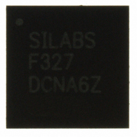
C8051F327-GM Silicon Laboratories Inc, C8051F327-GM Datasheet - Page 91

C8051F327-GM
Manufacturer Part Number
C8051F327-GM
Description
IC 8051 MCU FLASH 16K 28QFN
Manufacturer
Silicon Laboratories Inc
Series
C8051F32xr
Specifications of C8051F327-GM
Program Memory Type
FLASH
Program Memory Size
16KB (16K x 8)
Package / Case
28-QFN
Core Processor
8051
Core Size
8-Bit
Speed
25MHz
Connectivity
UART/USART, USB
Peripherals
POR
Number Of I /o
15
Ram Size
1.5K x 8
Voltage - Supply (vcc/vdd)
2.7 V ~ 3.6 V
Oscillator Type
Internal
Operating Temperature
-40°C ~ 85°C
Processor Series
C8051F3x
Core
8051
Data Bus Width
8 bit
Data Ram Size
1.5 KB
Interface Type
UART/USB
Maximum Clock Frequency
25 MHz
Number Of Programmable I/os
15
Number Of Timers
2
Operating Supply Voltage
2.7 V to 3.6 V
Maximum Operating Temperature
+ 85 C
Mounting Style
SMD/SMT
3rd Party Development Tools
PK51, CA51, A51, ULINK2
Development Tools By Supplier
C8051F326DK
Minimum Operating Temperature
- 40 C
Package
28QFN EP
Device Core
8051
Family Name
C8051F327
Maximum Speed
25 MHz
Lead Free Status / RoHS Status
Lead free / RoHS Compliant
For Use With
336-1481 - DAUGHTER CARD TOOLSTCK C8051F327770-1006 - ISP 4PORT FOR SILABS C8051F MCU
Eeprom Size
-
Data Converters
-
Lead Free Status / Rohs Status
Lead free / RoHS Compliant
Other names
336-1297-5
Available stocks
Company
Part Number
Manufacturer
Quantity
Price
Part Number:
C8051F327-GM
Manufacturer:
SILICON LABS/èٹ¯ç§‘
Quantity:
20 000
Bits7:
Bit6:
Bits5–0: USBADDR: USB0 Indirect Register Address
BUSY
R/W
Bit7
USB Register Definition 12.2. USB0ADR: USB0 Indirect Address
BUSY: USB0 Register Read Busy Flag
This bit is used during indirect USB0 register accesses. Software should write ‘1’ to this bit to
initiate a read of the USB0 register targeted by the USBADDR bits (USB0ADR.[5-0]). The
target address and BUSY bit may be written in the same write to USB0ADR. After BUSY is
set to ‘1’, hardware will clear BUSY when the targeted register data is ready in the
USB0DAT register. Software should check BUSY for ‘0’ before writing to USB0DAT.
Write:
0: No effect.
1: A USB0 indirect register read is initiated at the address specified by the USBADDR bits.
Read:
0: USB0DAT register data is valid.
1: USB0 is busy accessing an indirect register; USB0DAT register data is invalid.
AUTORD: USB0 Register Auto-read Flag
This bit is used for block FIFO reads.
0: BUSY must be written manually for each USB0 indirect register read.
1: The next indirect register read will automatically be initiated when software reads
USB0DAT (USBADDR bits will not be changed).
These bits hold a 6-bit address used to indirectly access the USB0 core registers. Table 12.2
lists the USB0 core registers and their indirect addresses. Reads and writes to USB0DAT
will target the register indicated by the USBADDR bits.
AUTORD
R/W
Bit6
R/W
Bit5
R/W
Bit4
Rev. 1.1
R/W
Bit3
USBADDR
R/W
Bit2
R/W
Bit1
C8051F326/7
R/W
Bit0
SFR Address:
00000000
Reset Value
0x96
91


