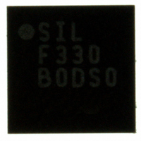
C8051F330-GM Silicon Laboratories Inc, C8051F330-GM Datasheet - Page 58

C8051F330-GM
Manufacturer Part Number
C8051F330-GM
Description
IC 8051 MCU 8K FLASH 20MLP
Manufacturer
Silicon Laboratories Inc
Series
C8051F33xr
Specifications of C8051F330-GM
Program Memory Type
FLASH
Program Memory Size
8KB (8K x 8)
Package / Case
20-QFN
Core Processor
8051
Core Size
8-Bit
Speed
25MHz
Connectivity
SMBus (2-Wire/I²C), SPI, UART/USART
Peripherals
POR, PWM, Temp Sensor, WDT
Number Of I /o
17
Ram Size
768 x 8
Voltage - Supply (vcc/vdd)
2.7 V ~ 3.6 V
Data Converters
A/D 16x10b; D/A 1x10b
Oscillator Type
Internal
Operating Temperature
-40°C ~ 85°C
Processor Series
C8051F3x
Core
8051
Data Bus Width
8 bit
Data Ram Size
768 B
Interface Type
I2C/SMBus/SPI/UART
Maximum Clock Frequency
25 MHz
Number Of Programmable I/os
17
Number Of Timers
4
Operating Supply Voltage
2.7 V to 3.6 V
Maximum Operating Temperature
+ 85 C
Mounting Style
SMD/SMT
3rd Party Development Tools
KSK-SL-TOOLSTICK, PK51, CA51, A51, ULINK2
Development Tools By Supplier
C8051F330DK
Minimum Operating Temperature
- 40 C
On-chip Adc
16-ch x 10-bit
On-chip Dac
1-ch x 10-bit
No. Of I/o's
17
Ram Memory Size
768Byte
Cpu Speed
25MHz
No. Of Timers
4
Rohs Compliant
Yes
Lead Free Status / RoHS Status
Lead free / RoHS Compliant
For Use With
336-1541 - KIT TOOL EVAL SYS IN A USB STICK770-1006 - ISP 4PORT FOR SILABS C8051F MCU336-1451 - ADAPTER PROGRAM TOOLSTICK F330336-1346 - DAUGHTER CARD TOOLSTICK F330336-1264 - DEV KIT FOR C8051F330/F331
Eeprom Size
-
Lead Free Status / Rohs Status
Lead free / RoHS Compliant
Other names
336-1262
Available stocks
Company
Part Number
Manufacturer
Quantity
Price
Company:
Part Number:
C8051F330-GM
Manufacturer:
SiliconL
Quantity:
6 420
Company:
Part Number:
C8051F330-GM
Manufacturer:
SILICON
Quantity:
121
Part Number:
C8051F330-GM
Manufacturer:
SILICON LABS/èٹ¯ç§‘
Quantity:
20 000
Company:
Part Number:
C8051F330-GM-15T
Manufacturer:
SILICON
Quantity:
3 741
Part Number:
C8051F330-GMR
Manufacturer:
SILICON LABS/èٹ¯ç§‘
Quantity:
20 000
7.
The Voltage reference MUX on the C8051F330/2/4 devices is configurable to use an externally connected
voltage reference, the internal reference voltage generator, or the V
Figure 7.1). The REFSL bit in the Reference Control register (REF0CN) selects the reference source. For
an external source or the internal reference, REFSL should be set to ‘0’. To use V
source, REFSL should be set to ‘1’.
The BIASE bit enables the internal voltage bias generator, which is used by the ADC, Temperature Sensor,
internal oscillators, and Current DAC. This bias is enabled when any of the aforementioned peripherals are
enabled. The bias generator may be enabled manually by writing a ‘1’ to the BIASE bit in register
REF0CN; see SFR Definition 7.1 for REF0CN register details. The electrical specifications for the voltage
reference circuit are given in Table 7.1.
The internal voltage reference circuit consists of a 1.2 V, temperature stable bandgap voltage reference
generator and a gain-of-two output buffer amplifier. The internal voltage reference can be driven out on the
VREF pin by setting the REFBE bit in register REF0CN to a ‘1’ (see SFR Definition 7.1). The maximum
load seen by the VREF pin must be less than 200 µA to GND. When using the internal voltage reference,
bypass capacitors of 0.1 µF and 4.7 µF are recommended from the VREF pin to GND. If the internal refer-
ence is not used, the REFBE bit should be cleared to ‘0’. Electrical specifications for the internal voltage
reference are given in Table 7.1.
Important Note about the VREF Pin: Port pin P0.0 is used as the external VREF input and as an output
for the internal VREF. When using either an external voltage reference or the internal reference circuitry,
P0.0 should be configured as an analog pin, and skipped by the Digital Crossbar. To configure P0.0 as an
analog pin, set to ‘0’ Bit0 in register P0MDIN. To configure the Crossbar to skip P0.0, set Bit 0 in register
P0SKIP to ‘1’. Refer to
details. The TEMPE bit in register REF0CN enables/disables the temperature sensor. While disabled, the
temperature sensor defaults to a high impedance state and any ADC0 measurements performed on the
sensor result in meaningless data.
Voltage Reference (C8051F330/2/4 only)
VDD
GND
4.7F
Recommended Bypass
Figure 7.1. Voltage Reference Functional Block Diagram
R1
Capacitors
+
Section “14. Port Input/Output” on page 123
Reference
External
Voltage
Circuit
0.1F
VREF
VDD
REF0CN
Rev. 1.7
0
1
IOSCE
N
Reference
REFBE
Internal
EN
EN
EN
C8051F330/1/2/3/4/5
Bias Generator
Temp Sensor
for complete Port I/O configuration
DD
power supply voltage (see
To Analog Mux
(to ADC)
VREF
To ADC, IDAC,
Internal Oscillators
DD
as the reference
61


