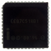
EE87C51RB1 Intel, EE87C51RB1 Datasheet - Page 4

EE87C51RB1
Manufacturer Part Number
EE87C51RB1
Description
IC MCU 8BIT 5V 16MHZ OTP 44PLCC
Manufacturer
Intel
Series
87Cr
Datasheet
1.EE87C51RB1.pdf
(20 pages)
Specifications of EE87C51RB1
Core Processor
MCS 51
Core Size
8-Bit
Speed
16MHz
Connectivity
SIO
Peripherals
WDT
Number Of I /o
32
Program Memory Size
16KB (16K x 8)
Program Memory Type
OTP
Ram Size
512 x 8
Voltage - Supply (vcc/vdd)
4 V ~ 6 V
Oscillator Type
External
Operating Temperature
-40°C ~ 85°C
Package / Case
44-PLCC
Lead Free Status / RoHS Status
Lead free / RoHS Compliant
Eeprom Size
-
Data Converters
-
Other names
864637
Available stocks
Company
Part Number
Manufacturer
Quantity
Price
Company:
Part Number:
EE87C51RB1
Manufacturer:
LT
Quantity:
101
Company:
Part Number:
EE87C51RB116
Manufacturer:
INTL
Quantity:
4 018
8XC51RA RB RC
PIN DESCRIPTIONS
V
V
V
reduce ground bounce and improve power supply
by-passing
This pin is not a substitute for the V
(Connection not necessary for proper operation )
Port 0 Port 0 is an 8-bit open drain bidirectional
I O port As an output port each pin can sink several
LS TTL inputs Port 0 pins that have 1’s written to
them float and in that state can be used as high-im-
pedance inputs
Port 0 is also the multiplexed low-order address and
data bus during accesses to external Program and
Data Memory In this application it uses strong inter-
nal pullups when emitting 1’s and can source and
sink several LS TTL inputs
Port 0 also receives the code bytes during EPROM
programming and outputs the code bytes during
program verification External pullup resistors are re-
quired during program verification
Port 1 Port 1 is an 8-bit bidirectional I O port with
internal pullups The Port 1 output buffers can drive
LS TTL inputs Port 1 pins that have 1’s written to
them are pulled high by the internal pullups and in
that state can be used as inputs As inputs Port 1
pins that are externally pulled low will source current
(I
ups
In addition Port 1 serves the functions of the follow-
ing special features of the 8XC51RX
Port 1 receives the low-order address bytes during
EPROM programming and verifying
Port 2 Port 2 is an 8-bit bidirectional I O port with
internal pullups The Port 2 output buffers can drive
4
IL
CC
SS
SS1
Port Pin
P1 0
P1 1
on the data sheet) because of the internal pull-
Circuit ground
Supply voltage
Secondary ground (not on DIP) Provided to
T2 (External Count Input to Timer
Counter 2) Clock-Out
T2EX (Timer Counter 2 Capture
Reload Trigger and Direction Control)
Alternate Function
NOTE
SS
pin (pin 22)
LS TTL inputs Port 2 pins that have 1’s written to
them are pulled high by the internal pullups and in
that state can be used as inputs As inputs Port 2
pins that are externally pulled low will source current
(I
ups
Port 2 emits the high-order address byte during
fetches from external Program Memory and during
accesses to external Data Memory that use 16-bit
addresses (MOVX
uses strong internal pullups when emitting 1’s Dur-
ing accesses to external Data Memory that use 8-bit
addresses (MOVX
the P2 Special Function Register
Some Port 2 pins receive the high-order address bits
during EPROM programming and program verifica-
tion
Port 3 Port 3 is an 8-bit bidirectional I O port with
internal pullups The Port 3 output buffers can drive
LS TTL inputs Port 3 pins that have 1’s written to
them are pulled high by the internal pullups and in
that state can be used as inputs As inputs Port 3
pins that are externally pulled low will source current
(I
Port 3 also serves the functions of various special
features of the 8051 Family as listed below
RST Reset I O A high on this pin for two machine
cycles while the oscillator is running resets the de-
vice The port pins will be driven to their reset condi-
tion when a minimum V
the oscillator is running or not An internal pulldown
resistor permits a power-on reset with only a capaci-
tor connected to V
flow this RST pin will drive an output high pulse at a
minimum V
ternal reset signal is active
ALE Address Latch Enable output pulse for latching
the low byte of the address during accesses to ex-
Port Pin
IL
IL
P3 0
P3 1
P3 2
P3 3
P3 4
P3 5
P3 6
P3 7
on the data sheet) because of the internal pull-
on the data sheet) because of the pullups
OH2
RXD (serial input port)
TXD (serial output port)
INT0 (external interrupt 0)
INT1 (external interrupt 1)
T0 (Timer 0 external input)
T1 (Timer 1 external input)
WR (external data memory write strobe)
RD (external data memory read strobe)
for 96 x T
CC
Ri) Port 2 emits the contents of
Alternate Function
DPTR) In this application it
After a WatchDog Timer over-
IHI
OSC
voltage is applied whether
duration while the in-


