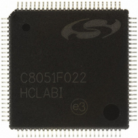
C8051F022-GQ Silicon Laboratories Inc, C8051F022-GQ Datasheet - Page 188

C8051F022-GQ
Manufacturer Part Number
C8051F022-GQ
Description
IC 8051 MCU 64K FLASH 100TQFP
Manufacturer
Silicon Laboratories Inc
Series
C8051F02xr
Specifications of C8051F022-GQ
Program Memory Type
FLASH
Program Memory Size
64KB (64K x 8)
Package / Case
100-TQFP, 100-VQFP
Core Processor
8051
Core Size
8-Bit
Speed
25MHz
Connectivity
EBI/EMI, SMBus (2-Wire/I²C), SPI, UART/USART
Peripherals
Brown-out Detect/Reset, POR, PWM, Temp Sensor, WDT
Number Of I /o
64
Ram Size
4.25K x 8
Voltage - Supply (vcc/vdd)
2.7 V ~ 3.6 V
Data Converters
A/D 8x8b, 8x10b; D/A 2x12b
Oscillator Type
Internal
Operating Temperature
-40°C ~ 85°C
Processor Series
C8051F0x
Core
8051
Data Bus Width
8 bit
Data Ram Size
4.25 KB
Interface Type
I2C/SMBus/SPI/UART
Maximum Clock Frequency
25 MHz
Number Of Programmable I/os
64
Number Of Timers
4
Operating Supply Voltage
2.7 V to 3.6 V
Maximum Operating Temperature
+ 85 C
Mounting Style
SMD/SMT
3rd Party Development Tools
PK51, CA51, A51, ULINK2
Development Tools By Supplier
C8051F020DK
Minimum Operating Temperature
- 40 C
On-chip Adc
8-ch x 8-bit or 8-ch x 10-bit
On-chip Dac
2-ch x 12-bit
No. Of I/o's
64
Ram Memory Size
4352Byte
Cpu Speed
25MHz
No. Of Timers
5
Rohs Compliant
Yes
Cpu Family
C8051F02x
Device Core
8051
Device Core Size
8b
Frequency (max)
25MHz
Total Internal Ram Size
4.25KB
# I/os (max)
64
Number Of Timers - General Purpose
5
Operating Supply Voltage (typ)
3.3V
Operating Supply Voltage (max)
3.6V
Operating Supply Voltage (min)
2.7V
Instruction Set Architecture
CISC
Operating Temp Range
-40C to 85C
Operating Temperature Classification
Industrial
Mounting
Surface Mount
Pin Count
100
Package Type
TQFP
Lead Free Status / RoHS Status
Lead free / RoHS Compliant
For Use With
336-1200 - DEV KIT FOR F020/F021/F022/F023
Eeprom Size
-
Lead Free Status / Rohs Status
Lead free / RoHS Compliant
Other names
336-1202
Available stocks
Company
Part Number
Manufacturer
Quantity
Price
Company:
Part Number:
C8051F022-GQ
Manufacturer:
Silicon Laboratories Inc
Quantity:
10 000
Part Number:
C8051F022-GQ
Manufacturer:
SILICON LABS/èٹ¯ç§‘
Quantity:
20 000
Company:
Part Number:
C8051F022-GQR
Manufacturer:
Silicon Laboratories Inc
Quantity:
10 000
C8051F020/1/2/3
18.3.3. Slave Transmitter Mode
Serial data is transmitted on SDA while the serial clock is received on SCL. The SMBus0 interface receives a START
followed by data byte containing the slave address and direction bit. If the received slave address matches the address
held in register SMB0ADR, the SMBus0 interface generates an ACK. SMBus0 will also ACK if the general call
address (0x00) is received and the General Call Address Enable bit (SMB0ADR.0) is set to logic 1. In this case the
data direction bit (R/W) will be logic 1 to indicate a "READ" operation. The SMBus0 interface receives the clock on
SCL and transmits one or more bytes of serial data, waiting for an ACK from the master after each byte. SMBus0
exits slave mode after receiving a STOP condition from the master.
18.3.4. Slave Receiver Mode
Serial data is received on SDA while the serial clock is received on SCL. The SMBus0 interface receives a START
followed by data byte containing the slave address and direction bit. If the received slave address matches the address
held in register SMB0ADR, the interface generates an ACK. SMBus0 will also ACK if the general call address
(0x00) is received and the General Call Address Enable bit (SMB0ADR.0) is set to logic 1. In this case the data direc-
tion bit (R/W) will be logic 0 to indicate a "WRITE" operation. The SMBus0 interface receives one or more bytes of
serial data; after each byte is received, the interface transmits an ACK or NACK depending on the state of the AA bit
in SMB0CN. SMBus0 exits Slave Receiver Mode after receiving a STOP condition from the master.
188
S
S
Received by SMBus
Interface
Transmitted by
SMBus Interface
Received by SMBus
Interface
Transmitted by
SMBus Interface
SLA
SLA
Figure 18.6. Typical Slave Transmitter Sequence
Figure 18.7. Typical Slave Receiver Sequence
Interrupt
W
R
Interrupt
A
A
Data Byte
Data Byte
Rev. 1.4
Interrupt
Interrupt
A
A
S = START
P = STOP
N = NACK
W = WRITE
SLA = Slave Address
S = START
P = STOP
A = ACK
R = READ
SLA = Slave Address
Data Byte
Data Byte
Interrupt
Interrupt
N
A
Interrupt
Interrupt
P
P


