MAXQ7667AACM/V+ Maxim Integrated Products, MAXQ7667AACM/V+ Datasheet - Page 12
MAXQ7667AACM/V+
Manufacturer Part Number
MAXQ7667AACM/V+
Description
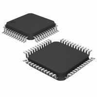
IC MCU-BASED DAS 16BIT 48-LQFP
Manufacturer
Maxim Integrated Products
Series
MAXQ™r
Datasheet
1.MAXQ7667AACMV.pdf
(40 pages)
Specifications of MAXQ7667AACM/V+
Core Processor
RISC
Core Size
16-Bit
Speed
16MHz
Connectivity
LIN, SPI, UART/USART
Peripherals
Brown-out Detect/Reset, POR, WDT
Number Of I /o
16
Program Memory Size
32KB (16K x 16)
Program Memory Type
FLASH
Ram Size
2K x 16
Voltage - Supply (vcc/vdd)
2.25 V ~ 2.75 V
Data Converters
A/D 5x12b
Oscillator Type
Internal
Operating Temperature
-40°C ~ 125°C
Package / Case
48-LQFP
Processor Series
MAXQ7667
Core
RISC
Data Bus Width
16 bit
Data Ram Size
4 KB
Interface Type
UART, JTAG, LIN
Maximum Clock Frequency
16 MHz
Number Of Programmable I/os
16
Number Of Timers
3
Operating Supply Voltage
5 V
Maximum Operating Temperature
+ 125 C
Mounting Style
SMD/SMT
Development Tools By Supplier
MAXQ7667EVKIT
Minimum Operating Temperature
- 40 C
On-chip Adc
12 bit, 5 Channel
Lead Free Status / RoHS Status
Lead free / RoHS Compliant
Eeprom Size
-
Lead Free Status / Rohs Status
Details


16-Bit, RISC, Microcontroller-Based,
Ultrasonic Distance-Measuring System
12
6, 19, 42
7, 18, 43
8, 17, 44
PIN
10
11
12
13
14
15
16
20
______________________________________________________________________________________
1
2
3
4
5
9
P1.7/SYNC/SS
P1.4/MOSI
P1.5/MISO
P1.6/SCLK
P0.2/
P1.3/TCK
P0.0/URX
P0.1/UTX
P0.4/T0B
P0.7/T2B
ADCCTL
DVDDIO
P0.3/T0/
P0.5/T1
P0.6/T2
NAME
DGND
DVDD
XIN
Port 1 Data 3/JTAG Serial Clock Input. P1.3 is a general-purpose digital I/O. TCK is the JTAG
serial test clock input. Refer to the MAXQ7667 User’s Guide Sections 5 and 11.
Port 1 Data 4/SPI Serial Data Output. P1.4 is a general-purpose digital I/O. MOSI is the master
output, slave input for the SPI interface. Refer to the MAXQ7667 User’s Guide Sections 5 and 9.
Port 1 Data 5/SPI Serial Data Input. P1.5 is a general-purpose digital I/O. MISO is the master input,
slave output for the SPI interface. Refer to the MAXQ7667 User’s Guide Sections 5 and 9.
Port 1 Data 6/SPI Serial Clock Output. P1.6 is a general-purpose digital I/O. SCLK is the serial
clock for the SPI interface. SCLK is an input when operating as a slave and an output when
operating as a master. Refer to the MAXQ7667 User’s Guide Sections 5 and 9.
Port 1 Data 7/Schedule Timer Sync Input/SPI Slave Select. P1.7 is a general-purpose digital I/O.
A rising edge on the SYNC input resets the schedule timer. In SPI slave mode, SS is the SPI
slave-select input. In SPI master mode, use SS or a GPIO to manually select an external slave.
Refer to the MAXQ7667 User’s Guide Sections 5, 7, and 9.
Digital Supply Voltage. Connect DVDD directly to a +2.5V external source or to REG2P5 output for
single supply operation. Bypass DVDD to DGND with a 0.1µF capacitor as close as possible to
the device. Connect all DVDD nodes together.
Digital Ground. Connect all DGND nodes together. Connect to AGND at a single point.
Digital I/O Supply Voltage. DVDDIO powers all digital I/Os except for XIN and XOUT. Bypass
DVDDIO to DGND with a 0.1µF capacitor as close as possible to the device. Connect all DVDDIO
nodes together.
Port 0 Data 0/UART Receive Data Input. P0.0 is a general-purpose digital I/O. URX is a UART or
LIN data receive input. Refer to the MAXQ7667 User’s Guide Sections 5 and 8.
Port 0 Data 1/UART Transmit Data Output. P0.1 is a general-purpose digital I/O. UTX is a UART or
LIN data transmit output. Refer to the MAXQ7667 User’s Guide Sections 5 and 8.
Port 0 Data 2/UART Transmit Output. P0.2 is a general-purpose digital I/O.
the UART is transmitting. Use
MAXQ7667 User’s Guide Sections 5 and 8.
Port 0 Data 3/Timer 0 I/O/ADC Control Input. P0.3 is a general-purpose digital I/O. T0 is the
primary Type 2 timer/counter 0 output or input. ADCCTL is a sampling/conversion trigger input for
the SAR ADC. Refer to the MAXQ7667 User’s Guide Sections 5, 6, and 14.
Port 0 Data 4/Timer 0B I/O/Comparator Output. P0.4 is a general-purpose digital I/O. T0B is the
secondary Type 2 timer/counter 0 output or input. Refer to the MAXQ7667 User’s Guide Sections
5 and 6.
Port 0 Data 5/Timer 1 I/O. P0.5 is a general-purpose digital I/O. T1 is the primary Type 2
timer/counter 1 output or input. Refer to the MAXQ7667 User’s Guide Sections 5 and 6.
Port 0 Data 6/Timer 2 I/O. P0.6 is a general-purpose digital I/O. T2 is the primary Type 2
timer/counter 2 output or input. Refer to the MAXQ7667 User’s Guide Sections 5 and 6.
Port 0 Data 7/Timer 2B I/O. P0.7 is a general-purpose digital I/O. T2B is the secondary Type 2
timer/counter 2 output or input. Refer to the MAXQ7667 User’s Guide Sections 5 and 6.
Crystal Oscillator Input. Connect an external crystal or resonator between XIN and XOUT. When
using an external clock source drive XIN with 2.5V level clock while leaving XOUT unconnected.
Connect XIN to DGND when an external clock source is not used.
to enable an external LIN/UART transceiver. Refer to the
FUNCTION
Pin Description
asserts low when
Related parts for MAXQ7667AACM/V+
Image
Part Number
Description
Manufacturer
Datasheet
Request
R

Part Number:
Description:
16-bit, Risc, Microcontroller-based, Ultrasonic Distance-measuring System
Manufacturer:
Maxim Integrated Products, Inc.
Datasheet:

Part Number:
Description:
MAX7528KCWPMaxim Integrated Products [CMOS Dual 8-Bit Buffered Multiplying DACs]
Manufacturer:
Maxim Integrated Products
Datasheet:
Part Number:
Description:
Single +5V, fully integrated, 1.25Gbps laser diode driver.
Manufacturer:
Maxim Integrated Products
Datasheet:
Part Number:
Description:
Single +5V, fully integrated, 155Mbps laser diode driver.
Manufacturer:
Maxim Integrated Products
Datasheet:
Part Number:
Description:
VRD11/VRD10, K8 Rev F 2/3/4-Phase PWM Controllers with Integrated Dual MOSFET Drivers
Manufacturer:
Maxim Integrated Products
Datasheet:
Part Number:
Description:
Highly Integrated Level 2 SMBus Battery Chargers
Manufacturer:
Maxim Integrated Products
Datasheet:
Part Number:
Description:
Current Monitor and Accumulator with Integrated Sense Resistor; ; Temperature Range: -40°C to +85°C
Manufacturer:
Maxim Integrated Products
Part Number:
Description:
TSSOP 14/A�/RS-485 Transceivers with Integrated 100O/120O Termination Resis
Manufacturer:
Maxim Integrated Products
Part Number:
Description:
TSSOP 14/A�/RS-485 Transceivers with Integrated 100O/120O Termination Resis
Manufacturer:
Maxim Integrated Products
Part Number:
Description:
QFN 16/A�/AC-DC and DC-DC Peak-Current-Mode Converters with Integrated Step
Manufacturer:
Maxim Integrated Products
Part Number:
Description:
TDFN/A/65V, 1A, 600KHZ, SYNCHRONOUS STEP-DOWN REGULATOR WITH INTEGRATED SWI
Manufacturer:
Maxim Integrated Products
Part Number:
Description:
Integrated Temperature Controller f
Manufacturer:
Maxim Integrated Products
Part Number:
Description:
SOT23-6/I�/45MHz to 650MHz, Integrated IF VCOs with Differential Output
Manufacturer:
Maxim Integrated Products
Part Number:
Description:
SOT23-6/I�/45MHz to 650MHz, Integrated IF VCOs with Differential Output
Manufacturer:
Maxim Integrated Products
Part Number:
Description:
EVALUATION KIT/2.4GHZ TO 2.5GHZ 802.11G/B RF TRANSCEIVER WITH INTEGRATED PA
Manufacturer:
Maxim Integrated Products