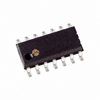
PIC16F610-I/SL Microchip Technology, PIC16F610-I/SL Datasheet - Page 69

PIC16F610-I/SL
Manufacturer Part Number
PIC16F610-I/SL
Description
IC PIC MCU FLASH 1KX14 14SOIC
Manufacturer
Microchip Technology
Series
PIC® 16Fr
Datasheets
1.PIC12F609T-ISN.pdf
(26 pages)
2.PIC16F616T-ISL.pdf
(214 pages)
3.PIC16F616T-ISL.pdf
(8 pages)
4.PIC16F616-ESL.pdf
(180 pages)
Specifications of PIC16F610-I/SL
Program Memory Type
FLASH
Program Memory Size
1.75KB (1K x 14)
Package / Case
14-SOIC (3.9mm Width), 14-SOL
Core Processor
PIC
Core Size
8-Bit
Speed
20MHz
Peripherals
Brown-out Detect/Reset, POR, PWM, WDT
Number Of I /o
11
Ram Size
64 x 8
Voltage - Supply (vcc/vdd)
2 V ~ 5.5 V
Oscillator Type
Internal
Operating Temperature
-40°C ~ 85°C
Processor Series
PIC16F
Core
PIC
Data Bus Width
8 bit
Data Ram Size
64 B
Interface Type
RS-232 / USB
Maximum Clock Frequency
20 MHz
Number Of Programmable I/os
11
Number Of Timers
2
Maximum Operating Temperature
+ 85 C
Mounting Style
SMD/SMT
3rd Party Development Tools
52715-96, 52716-328, 52717-734
Development Tools By Supplier
PG164130, DV164035, DV244005, DV164005, PG164120, ICE2000
Minimum Operating Temperature
- 40 C
Lead Free Status / RoHS Status
Lead free / RoHS Compliant
For Use With
AC162083 - HEADER MPLAB ICD2 PIC16F616 8/14
Eeprom Size
-
Data Converters
-
Connectivity
-
Lead Free Status / Rohs Status
Lead free / RoHS Compliant
Available stocks
Company
Part Number
Manufacturer
Quantity
Price
Company:
Part Number:
PIC16F610-I/SL
Manufacturer:
WELTREND
Quantity:
340
Company:
Part Number:
PIC16F610-I/SL
Manufacturer:
Microchip Technology
Quantity:
1 968
Part Number:
PIC16F610-I/SL
Manufacturer:
MIC
Quantity:
20 000
REGISTER 8-4:
REGISTER 8-5:
© 2007 Microchip Technology Inc.
bit 7
Legend:
R = Readable bit
-n = Value at POR
bit 7
bit 6
bit 5
bit 4
bit 3
bit 2
bit 1
bit 0
Note 1:
bit 7
Legend:
R = Readable bit
-n = Value at POR
bit 7-6
bit 5-0
SRCS1
SR1
R/W-0
R/W-0
2:
(2)
The C1OUT and C2OUT bits in the CMxCON0 register will always reflect the actual comparator output (not the level on
the pin), regardless of the SR latch operation.
To enable an SR Latch output to the pin, the appropriate CxOE, and TRIS bits must be properly configured.
SR1: SR Latch Configuration bit
1 =
0 =
SR0: SR Latch Configuration bits
1 =
0 =
C1SEN: C1 Set Enable bit
1 = C1 comparator output sets SR latch
0 = C1 comparator output has no effect on SR latch
C2REN: C2 Reset Enable bit
1 = C2 comparator output resets SR latch
0 = C2 comparator output has no effect on SR latch
PULSS: Pulse the SET Input of the SR Latch bit
1 = Triggers pulse generator to set SR latch. Bit is immediately reset by hardware.
0 = Does not trigger pulse generator
PULSR: Pulse the Reset Input of the SR Latch bit
1 = Triggers pulse generator to reset SR latch. Bit is immediately reset by hardware.
0 = Does not trigger pulse generator
Unimplemented: Read as ‘0’
SRCLKEN: SR Latch Set Clock Enable bit
1 = Set input of SR latch is pulsed with SRCLK
0 = Set input of SR latch is not pulsed with the SRCLK
SRCS<1:0>: SR Latch Clock Prescale bits
00 = F
01 = F
10 = F
11 = F
Unimplemented: Read as ‘0’
SRCS0
SR0
R/W-0
R/W-0
C2OUT pin is the latch Q output
C2OUT pin is the C2 comparator output
C1OUT pin is the latch Q output
C1OUT pin is the C1 Comparator output
SRCON0: SR LATCH CONTROL 0 REGISTER
SRCON1: SR LATCH CONTROL 1 REGISTER
OSC
OSC
OSC
OSC
(2)
/16
/32
/64
/128
W = Writable bit
‘1’ = Bit is set
W = Writable bit
‘1’ = Bit is set
C1SEN
R/W-0
U-0
—
PIC16F610/616/16HV610/616
(2)
(2)
C2REN
R/W-0
U-0
Preliminary
—
S = Bit is set only -
U = Unimplemented bit, read as ‘0’
‘0’ = Bit is cleared
S = Bit is set only -
U = Unimplemented bit, read as ‘0’
‘0’ = Bit is cleared
PULSS
R/S-0
U-0
—
PULSR
R/S-0
U-0
—
x = Bit is unknown
x = Bit is unknown
U-0
U-0
—
—
DS41288C-page 67
SRCLKEN
R/W-0
U-0
—
bit 0
bit 0


