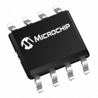
PIC12F617-I/MS Microchip Technology, PIC12F617-I/MS Datasheet - Page 47

PIC12F617-I/MS
Manufacturer Part Number
PIC12F617-I/MS
Description
IC MCU 8BIT 3.5KB FLASH 8MSOP
Manufacturer
Microchip Technology
Series
PIC® 12Fr
Datasheets
1.PIC12F609T-ISN.pdf
(212 pages)
2.PIC12F609T-ISN.pdf
(8 pages)
3.PIC12F617-IP.pdf
(4 pages)
Specifications of PIC12F617-I/MS
Core Size
8-Bit
Program Memory Size
3.5KB (2K x 14)
Core Processor
PIC
Speed
20MHz
Peripherals
Brown-out Detect/Reset, POR, PWM, WDT
Number Of I /o
5
Program Memory Type
FLASH
Ram Size
128 x 8
Voltage - Supply (vcc/vdd)
2 V ~ 5.5 V
Data Converters
A/D 4x10b
Oscillator Type
Internal
Operating Temperature
-40°C ~ 85°C
Package / Case
8-MSOP, Micro8™, 8-uMAX, 8-uSOP,
Controller Family/series
PIC12
Ram Memory Size
128Byte
Cpu Speed
20MHz
No. Of Timers
3
No. Of Pwm Channels
1
Digital Ic Case Style
MSOP
Processor Series
PIC12F
Core
PIC
Data Bus Width
8 bit
Data Ram Size
128 KB
Maximum Clock Frequency
8 MHz
Number Of Programmable I/os
6
Number Of Timers
3
Operating Supply Voltage
2 V to 5.5 V
Maximum Operating Temperature
+ 85 C
Mounting Style
SMD/SMT
3rd Party Development Tools
52715-96, 52716-328, 52717-734
Development Tools By Supplier
PG164130, DV164035, DV244005, DV164005, ICE2000
Minimum Operating Temperature
- 40 C
On-chip Adc
10 bit, 4 Channel
Lead Free Status / RoHS Status
Lead free / RoHS Compliant
Eeprom Size
-
Connectivity
-
Lead Free Status / Rohs Status
Details
- Current page: 47 of 212
- Download datasheet (2Mb)
5.2.4
Each GPIO pin is multiplexed with other functions. The
pins and their combined functions are briefly described
here. For specific information about individual functions
such as the Comparator or the ADC, refer to the
appropriate section in this data sheet.
5.2.4.1
Figure 5-1 shows the diagram for this pin. The GP0 pin
is configurable to function as one of the following:
• a general purpose I/O
• an analog input for the ADC
• an analog non-inverting input to the comparator
• a PWM output
• In-Circuit Serial Programming data
FIGURE 5-1:
2010 Microchip Technology Inc.
Interrupt-on-
Change
Note 1:
Write ‘0’ to GBIF
PIN DESCRIPTIONS AND
DIAGRAMS
GP0/AN0
2:
3:
(1)
Comparator mode and ANSEL determines Analog Input mode.
Set has priority over Reset.
PIC12F615/617/HV615 only.
Q
BLOCK DIAGRAM OF GP<1:0>
S
R
(1)
(2)
/CIN+/P1B
Data Bus
(1)
TRISIO
WPU
GPIO
WPU
TRISIO
GPIO
From other
GP<5:0> pins (GP0)
GP<5:2, 0> pins (GP1)
WR
RD
PIC12F609/615/617/12HV609/615
WR
WR
WR
IOC
IOC
RD
RD
RD
(1)
D
D
D
D
/ICSPDAT
CK
CK
CK
CK
Q
Q
Q
Q
Q
Q
Q
Q
To A/D Converter
To Comparator
5.2.4.2
Figure 5-1 shows the diagram for this pin. The GP1 pin
is configurable to function as one of the following:
• a general purpose I/O
• an analog input for the ADC
• an analog inverting input to the comparator
• a voltage reference input for the ADC
• In-Circuit Serial Programming clock
RD GPIO
Input Mode
Analog
Note 1:
(3)
Q
Q
(1)
Input Mode
Analog
EN
EN
D
D
PIC12F615/617/HV615 only.
GP1/AN1
(1)
GPPU
Q1
(1)
/CIN0-/V
V
Weak
DD
(1)
REF
DS41302D-page 47
(1)
V
V
(1)
DD
SS
/ICSPCLK
I/O Pin
Related parts for PIC12F617-I/MS
Image
Part Number
Description
Manufacturer
Datasheet
Request
R

Part Number:
Description:
IC MCU 8BIT 3.5KB FLASH 8DIP
Manufacturer:
Microchip Technology
Datasheet:

Part Number:
Description:
MCU 8BIT 3.5KB R/W FLASH 8DFN
Manufacturer:
Microchip Technology
Datasheet:

Part Number:
Description:
IC MCU 8BIT 3.5KB FLASH 8SOIC
Manufacturer:
Microchip Technology
Datasheet:

Part Number:
Description:
IC MCU 8BIT 3.5KB FLASH 8DFN
Manufacturer:
Microchip Technology
Datasheet:

Part Number:
Description:
MCU 8BIT 3.5KB R/W FLASH 8MSOP
Manufacturer:
Microchip Technology
Datasheet:

Part Number:
Description:
MCU 8BIT 3.5KB R/W FLASH 8PDIP
Manufacturer:
Microchip Technology
Datasheet:

Part Number:
Description:
3.5KB Self Read/Write Flash, 128B RAM, 6 I/O, 8MHz Internal Oscillator 8 SOIC 3.
Manufacturer:
Microchip Technology
Datasheet:

Part Number:
Description:
7 KB Flash, 256 Bytes RAM, 32 MHz Int. Osc, 6 I/0, Enhanced Mid Range Core 8 PDI
Manufacturer:
Microchip Technology
Datasheet:

Part Number:
Description:
7 KB Flash, 256 Bytes RAM, 32 MHz Int. Osc, 6 I/0, Enhanced Mid Range Core, Nano
Manufacturer:
Microchip Technology
Datasheet:

Part Number:
Description:
7 KB Flash, 256 Bytes RAM, 32 MHz Int. Osc, 6 I/0, Enhanced Mid Range Core 8 DFN
Manufacturer:
Microchip Technology

Part Number:
Description:
7 KB Flash, 256 Bytes RAM, 32 MHz Int. Osc, 6 I/0, Enhanced Mid Range Core 8 SOI
Manufacturer:
Microchip Technology

Part Number:
Description:
7 KB Flash, 256 Bytes RAM, 32 MHz Int. Osc, 6 I/0, Enhanced Mid Range Core, Nano
Manufacturer:
Microchip Technology
Datasheet:

Part Number:
Description:
7 KB Flash, 256 Bytes RAM, 32 MHz Int. Osc, 6 I/0, Enhanced Mid Range Core, Nano
Manufacturer:
Microchip Technology
Datasheet:

Part Number:
Description:
7 KB Flash, 256 Bytes RAM, 32 MHz Int. Osc, 6 I/0, Enhanced Mid Range Core, Nano
Manufacturer:
Microchip Technology
Datasheet:

Part Number:
Description:
7 KB Flash, 256 Bytes RAM, 32 MHz Int. Osc, 6 I/0, Enhanced Mid Range Core, Nano
Manufacturer:
Microchip Technology


