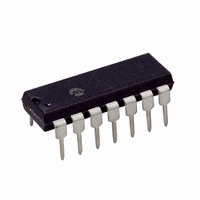
PIC16F684-E/P Microchip Technology, PIC16F684-E/P Datasheet - Page 65

PIC16F684-E/P
Manufacturer Part Number
PIC16F684-E/P
Description
IC PIC MCU FLASH 2KX14 14DIP
Manufacturer
Microchip Technology
Series
PIC® 16Fr
Datasheets
1.PIC16F616T-ISL.pdf
(8 pages)
2.PIC16F688T-ISL.pdf
(688 pages)
3.PIC16F684-ISL.pdf
(4 pages)
4.PIC16F684-ISL.pdf
(192 pages)
5.PIC16F684-ISL.pdf
(6 pages)
6.PIC16F684-IST.pdf
(164 pages)
Specifications of PIC16F684-E/P
Program Memory Type
FLASH
Program Memory Size
3.5KB (2K x 14)
Package / Case
14-DIP (0.300", 7.62mm)
Core Processor
PIC
Core Size
8-Bit
Speed
20MHz
Peripherals
Brown-out Detect/Reset, POR, PWM, WDT
Number Of I /o
12
Eeprom Size
256 x 8
Ram Size
128 x 8
Voltage - Supply (vcc/vdd)
2 V ~ 5.5 V
Data Converters
A/D 8x10b
Oscillator Type
Internal
Operating Temperature
-40°C ~ 125°C
Processor Series
PIC16F
Core
PIC
Data Bus Width
8 bit
Data Ram Size
128 B
Maximum Clock Frequency
20 MHz
Number Of Programmable I/os
12
Number Of Timers
3
Operating Supply Voltage
2 V to 5.5 V
Maximum Operating Temperature
+ 125 C
Mounting Style
Through Hole
3rd Party Development Tools
52715-96, 52716-328, 52717-734
Development Tools By Supplier
PG164130, DV164035, DV244005, DV164005, PG164120, ICE2000, DM163014, DM164120-4
Minimum Operating Temperature
- 40 C
On-chip Adc
8-ch x 10-bit
Lead Free Status / RoHS Status
Lead free / RoHS Compliant
For Use With
DM163029 - BOARD PICDEM FOR MECHATRONICSACICE0207 - MPLABICE 14P 300 MIL ADAPTER
Connectivity
-
Lead Free Status / Rohs Status
Lead free / RoHS Compliant
8.10
The comparator voltage reference module provides an
internally generated voltage reference for the compara-
tors. The following features are available:
• Independent from Comparator operation
• Two 16-level voltage ranges
• Output clamped to V
• Ratiometric with V
The VRCON register (Register ) controls the voltage
reference module shown in Figure 8-8.
8.10.1
The comparator voltage reference is independent of
the comparator configuration. Setting the VREN bit of
the VRCON register will enable the voltage reference.
8.10.2
The
voltage levels in each range. Range selection is
controlled by the VRR bit of the VRCON register. The
16 levels are set with the VR<3:0> bits of the VRCON
register.
The CV
equations:
VRCON: VOLTAGE REFERENCE CONTROL REGISTER
© 2007 Microchip Technology Inc.
bit 7
Legend:
R = Readable bit
-n = Value at POR
bit 7
bit 6
bit 5
bit 4
bit 3-0
R/W-0
VREN
CV
REF
REF
Comparator Voltage Reference
INDEPENDENT OPERATION
OUTPUT VOLTAGE SELECTION
output voltage is determined by the following
voltage reference has 2 ranges with 16
VREN: CV
1 = CV
0 = CV
Unimplemented: Read as ‘0’
VRR: CV
1 = Low range
0 = High range
Unimplemented: Read as ‘0’
VR<3:0>: CV
When VRR = 1: CV
When VRR = 0: CV
DD
U-0
—
SS
REF
REF
REF
REF
circuit powered on
circuit powered down, no I
Range Selection bit
REF
W = Writable bit
‘1’ = Bit is set
Enable bit
Value Selection bits (0 ≤ VR<3:0> ≤ 15)
R/W-0
VRR
REF
REF
= (VR<3:0>/24) * V
= V
DD
/4 + (VR<3:0>/32) * V
U-0
—
DD
drain and CV
DD
U = Unimplemented bit, read as ‘0’
‘0’ = Bit is cleared
R/W-0
EQUATION 8-1:
The full range of V
the construction of the module. See Figure 8-8.
8.10.3
The CV
power consumption by configuring VRCON as follows:
• VREN = 0
• VRR = 1
• VR<3:0> = 0000
This allows the comparator to detect a zero-crossing
while not consuming additional CV
8.10.4
The comparator voltage reference is V
therefore, the CV
V
Voltage Reference can be found in Section 15.0
“Electrical Specifications”.
VR3
DD
V
V
. The tested absolute accuracy of the Comparator
DD
RR
RR
REF
REF
=
=
CV
CV
0 (high range):
1 (low range):
= V
OUTPUT CLAMPED TO V
OUTPUT RATIOMETRIC TO VDD
output voltage can be set to Vss with no
REF
REF
R/W-0
SS
VR2
REF
.
=
=
SS
output changes with fluctuations in
(VR<3:0>/24)
(V
to V
CV
DD
DD
/4) +
x = Bit is unknown
REF
PIC16F684
cannot be realized due to
R/W-0
VR1
OUTPUT VOLTAGE
(VR<3:0> V
REF
×
V
DS41202F-page 63
DD
module current.
DD
SS
×
derived and
R/W-0
VR0
DD
/32)
bit 0


