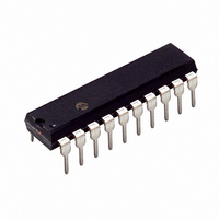
PIC16F631-E/P Microchip Technology, PIC16F631-E/P Datasheet - Page 106

PIC16F631-E/P
Manufacturer Part Number
PIC16F631-E/P
Description
IC PIC MCU FLASH 1KX14 20DIP
Manufacturer
Microchip Technology
Series
PIC® 16Fr
Datasheets
1.PIC16F616T-ISL.pdf
(8 pages)
2.PIC16F690DM-PCTLHS.pdf
(306 pages)
3.PIC16F677-IP.pdf
(2 pages)
4.PIC16F677-IP.pdf
(16 pages)
Specifications of PIC16F631-E/P
Core Processor
PIC
Core Size
8-Bit
Speed
20MHz
Peripherals
Brown-out Detect/Reset, POR, WDT
Number Of I /o
18
Program Memory Size
1.75KB (1K x 14)
Program Memory Type
FLASH
Eeprom Size
128 x 8
Ram Size
64 x 8
Voltage - Supply (vcc/vdd)
2 V ~ 5.5 V
Oscillator Type
Internal
Operating Temperature
-40°C ~ 125°C
Package / Case
20-DIP (0.300", 7.62mm)
For Use With
658-1047-5 - BOARD EVALUATION ACCESSTOUCHAC162061 - HEADER INTRFC MPLAB ICD2 20PINAC164039 - MODULE SKT PROMATE II 20DIP/SOICACICE0203 - MPLABICE 20P 300 MIL ADAPTER
Lead Free Status / RoHS Status
Lead free / RoHS Compliant
Data Converters
-
Connectivity
-
- PIC16F616T-ISL PDF datasheet
- PIC16F690DM-PCTLHS PDF datasheet #2
- PIC16F677-IP PDF datasheet #3
- PIC16F677-IP PDF datasheet #4
- Current page: 106 of 306
- Download datasheet (6Mb)
PIC16F631/677/685/687/689/690
8.10
The comparator voltage reference module provides an
internally generated voltage reference for the compara-
tors. The following features are available:
• Independent from Comparator operation
• Two 16-level voltage ranges
• Output clamped to V
• Ratiometric with V
• Fixed Reference (0.6)
The VRCON register (Register 8-5) controls the
Voltage Reference module shown in Figure 8-8.
8.10.1
The comparator voltage reference is independent of
the comparator configuration. Setting the VREN bit of
the VRCON register will enable the voltage reference.
8.10.2
The
voltage levels in each range. Range selection is
controlled by the VRR bit of the VRCON register. The
16 levels are set with the VR<3:0> bits of the VRCON
register.
The CV
equations:
EQUATION 8-1:
The full range of V
the construction of the module. See Figure 8-8.
DS41262E-page 104
V
V
CV
RR
RR
REF
REF
=
=
Comparator Voltage Reference
CV
CV
0 (high range):
1 (low range):
INDEPENDENT OPERATION
OUTPUT VOLTAGE SELECTION
output voltage is determined by the following
voltage reference has 2 ranges with 16
REF
REF
=
=
SS
DD
(VR<3:0>/24)
(V
to V
CV
SS
DD
DD
/4) +
REF
cannot be realized due to
OUTPUT VOLTAGE
(VR<3:0> V
×
V
DD
×
DD
/32)
8.10.3
The CV
power consumption by clearing the VP6EN bit of the
VRCON register.
This allows the comparator to detect a zero-crossing
while not consuming additional CV
8.10.4
The comparator voltage reference is V
therefore, the CV
V
Voltage Reference can be found in Section 17.0
“Electrical Specifications”.
DD
. The tested absolute accuracy of the Comparator
REF
OUTPUT CLAMPED TO V
OUTPUT RATIOMETRIC TO VDD
output voltage can be set to Vss with no
REF
output changes with fluctuations in
© 2008 Microchip Technology Inc.
REF
module current.
DD
SS
derived and
Related parts for PIC16F631-E/P
Image
Part Number
Description
Manufacturer
Datasheet
Request
R

Part Number:
Description:
3.5KB Flash, 128B RAM, 18 I/O, CLC, CWG, DDS, 10-bit ADC 20 QFN 4x4mm TUBE
Manufacturer:
Microchip Technology
Datasheet:

Part Number:
Description:
3.5KB Flash, 128B RAM, 18 I/O, CLC, CWG, DDS, 10-bit ADC 20 PDIP .300in TUBE
Manufacturer:
Microchip Technology
Datasheet:

Part Number:
Description:
3.5KB Flash, 128B RAM, 18 I/O, CLC, CWG, DDS, 10-bit ADC 20 SOIC .300in TUBE
Manufacturer:
Microchip Technology
Datasheet:

Part Number:
Description:
3.5KB Flash, 128B RAM, 18 I/O, CLC, CWG, DDS, 10-bit ADC 20 SSOP .209in TUBE
Manufacturer:
Microchip Technology
Datasheet:

Part Number:
Description:
3.5KB Flash, 128B RAM, 18 I/O, CLC, CWG, DDS, 10-bit ADC 20 QFN 4x4mm TUBE
Manufacturer:
Microchip Technology
Datasheet:

Part Number:
Description:
3.5KB Flash, 128B RAM, 18 I/O, CLC, CWG, DDS, 10-bit ADC 20 PDIP .300in TUBE
Manufacturer:
Microchip Technology
Datasheet:

Part Number:
Description:
3.5KB Flash, 128B RAM, 18 I/O, CLC, CWG, DDS, 10-bit ADC 20 SOIC .300in TUBE
Manufacturer:
Microchip Technology
Datasheet:

Part Number:
Description:
3.5KB Flash, 128B RAM, 18 I/O, CLC, CWG, DDS, 10-bit ADC 20 SSOP .209in TUBE
Manufacturer:
Microchip Technology
Datasheet:

Part Number:
Description:
3.5KB Flash, 128B RAM, 18 I/O, CLC, CWG, DDS, 10-bit ADC 20 QFN 4x4mm T/R
Manufacturer:
Microchip Technology
Datasheet:

Part Number:
Description:
3.5KB Flash, 128B RAM, 18 I/O, CLC, CWG, DDS, 10-bit ADC 20 SOIC .300in T/R
Manufacturer:
Microchip Technology
Datasheet:

Part Number:
Description:
3.5KB Flash, 128B RAM, 18 I/O, CLC, CWG, DDS, 10-bit ADC 20 SSOP .209in T/R
Manufacturer:
Microchip Technology
Datasheet:

Part Number:
Description:
3.5KB Flash, 128B RAM, 18 I/O, CLC, CWG, DDS, 10-bit ADC 20 QFN 4x4mm TUBE
Manufacturer:
Microchip Technology
Datasheet:

Part Number:
Description:
3.5KB Flash, 128B RAM, 18 I/O, CLC, CWG, DDS, 10-bit ADC 20 PDIP .300in TUBE
Manufacturer:
Microchip Technology
Datasheet:

Part Number:
Description:
3.5KB Flash, 128B RAM, 18 I/O, CLC, CWG, DDS, 10-bit ADC 20 SOIC .300in TUBE
Manufacturer:
Microchip Technology
Datasheet:

Part Number:
Description:
3.5KB Flash, 128B RAM, 18 I/O, CLC, CWG, DDS, 10-bit ADC 20 SSOP .209in TUBE
Manufacturer:
Microchip Technology
Datasheet:


