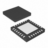
PIC16LF1826-I/MV Microchip Technology, PIC16LF1826-I/MV Datasheet - Page 179

PIC16LF1826-I/MV
Manufacturer Part Number
PIC16LF1826-I/MV
Description
IC MCU 8BIT FLASH 28UQFN
Manufacturer
Microchip Technology
Series
PIC® XLP™ 16Fr
Datasheet
1.PIC16F1826-IP.pdf
(406 pages)
Specifications of PIC16LF1826-I/MV
Core Size
8-Bit
Program Memory Size
3.5KB (2K x 14)
Core Processor
PIC
Speed
32MHz
Connectivity
I²C, SPI, UART/USART
Peripherals
Brown-out Detect/Reset, POR, PWM, WDT
Number Of I /o
16
Program Memory Type
FLASH
Eeprom Size
256 x 8
Ram Size
256 x 8
Voltage - Supply (vcc/vdd)
1.8 V ~ 3.6 V
Data Converters
A/D 12x10b
Oscillator Type
Internal
Operating Temperature
-40°C ~ 85°C
Package / Case
28-UFQFN Exposed Pad
Controller Family/series
PIC16LF
No. Of I/o's
16
Eeprom Memory Size
256Byte
Ram Memory Size
256Byte
Cpu Speed
32MHz
No. Of Timers
3
Processor Series
PIC16LF
Core
PIC
Data Ram Size
256 B
Maximum Clock Frequency
32 KHz
Number Of Programmable I/os
16
Number Of Timers
3
Operating Supply Voltage
1.8 V to 3.6 V
Maximum Operating Temperature
+ 125 C
3rd Party Development Tools
52715-96, 52716-328, 52717-734
Development Tools By Supplier
PG164130, DV164035, DV244005, DV164005
Minimum Operating Temperature
- 40 C
On-chip Adc
10 bit, 12 Channel
On-chip Dac
5 bit
Lead Free Status / RoHS Status
Lead free / RoHS Compliant
Lead Free Status / RoHS Status
Lead free / RoHS Compliant
- Current page: 179 of 406
- Download datasheet (4Mb)
20.0
The Timer1 module is a 16-bit timer/counter with the
following features:
• 16-bit timer/counter register pair (TMR1H:TMR1L)
• Programmable internal or external clock source
• 2-bit prescaler
• Dedicated 32 kHz oscillator circuit
• Optionally synchronized comparator out
• Multiple Timer1 gate (count enable) sources
• Interrupt on overflow
• Wake-up on overflow (external clock,
• Time base for the Capture/Compare function
• Special Event Trigger (with CCP/ECCP)
• Selectable Gate Source Polarity
FIGURE 20-1:
2010 Microchip Technology Inc.
Asynchronous mode only)
SYNCC1OUT
Comparator 1
Comparator 2
SYNCC2OUT
From Timer0
T1G
Overflow
T1GSS<1:0>
Note 1: ST Buffer is high speed type when using T1CKI.
TIMER1 MODULE WITH GATE
CONTROL
2: Timer1 register increments on rising edge.
3: Synchronize does not operate while in Sleep.
T1OSCEN
T1OSO
T1GPOL
T1CKI
T1OSI
Set flag bit
TMR1IF on
Overflow
00
10
11
TIMER1 BLOCK DIAGRAM
01
TMR1ON
T1GTM
T1OSC
TMR1H
EN
OUT
TMR1
(1)
T1G_IN
(2)
D
R
CK
TMR1L
Q
Q
1
0
Preliminary
TMR1CS<1:0>
Cap. Sensing
0
1
Oscillator
T1GGO/DONE
Q
Internal
Internal
F
OSC
Clock
Clock
F
OSC
EN
/4
D
• Gate Toggle Mode
• Gate Single-pulse Mode
• Gate Value Status
• Gate Event Interrupt
Figure 20-1 is a block diagram of the Timer1 module.
Single Pulse
Acq. Control
T1CLK
11
10
01
00
T1GSPM
PIC16F/LF1826/27
T1CKPS<1:0>
T1SYNC
Prescaler
1, 2, 4, 8
TMR1ON
0
1
To Clock Switching Modules
2
0
1
Internal
F
Clock
T1GVAL
OSC
TMR1GE
/2
Q1
Synchronized
Synchronize
Interrupt
clock input
D
EN
det
det
Sleep input
Q
(3)
To Comparator Module
DS41391C-page 179
Set
TMR1GIF
T1GCON
Data Bus
RD
Related parts for PIC16LF1826-I/MV
Image
Part Number
Description
Manufacturer
Datasheet
Request
R

Part Number:
Description:
IC, 8BIT MCU, PIC16LF, 32MHZ, QFN-28
Manufacturer:
Microchip Technology
Datasheet:

Part Number:
Description:
IC, 8BIT MCU, PIC16LF, 32MHZ, QFN-28
Manufacturer:
Microchip Technology
Datasheet:

Part Number:
Description:
IC, 8BIT MCU, PIC16LF, 32MHZ, DIP-18
Manufacturer:
Microchip Technology
Datasheet:

Part Number:
Description:
IC, 8BIT MCU, PIC16LF, 20MHZ, TQFP-44
Manufacturer:
Microchip Technology
Datasheet:

Part Number:
Description:
7 KB Flash, 384 Bytes RAM, 32 MHz Int. Osc, 16 I/0, Enhanced Mid Range Core, Nan
Manufacturer:
Microchip Technology

Part Number:
Description:
14KB Flash, 512B RAM, LCD, 11x10b ADC, EUSART, NanoWatt XLP 28 SOIC .300in T/R
Manufacturer:
Microchip Technology
Datasheet:

Part Number:
Description:
14KB Flash, 512B RAM, LCD, 11x10b ADC, EUSART, NanoWatt XLP 28 SSOP .209in T/R
Manufacturer:
Microchip Technology
Datasheet:

Part Number:
Description:
MCU PIC 14KB FLASH XLP 28-SSOP
Manufacturer:
Microchip Technology

Part Number:
Description:
MCU PIC 14KB FLASH XLP 28-SOIC
Manufacturer:
Microchip Technology

Part Number:
Description:
MCU PIC 512B FLASH XLP 28-UQFN
Manufacturer:
Microchip Technology

Part Number:
Description:
MCU PIC 14KB FLASH XLP 28-SPDIP
Manufacturer:
Microchip Technology

Part Number:
Description:
MCU 7KB FLASH 256B RAM 40-UQFN
Manufacturer:
Microchip Technology

Part Number:
Description:
MCU 7KB FLASH 256B RAM 44-TQFP
Manufacturer:
Microchip Technology

Part Number:
Description:
MCU 14KB FLASH 1KB RAM 28-UQFN
Manufacturer:
Microchip Technology

Part Number:
Description:
MCU PIC 14KB FLASH XLP 40-UQFN
Manufacturer:
Microchip Technology


