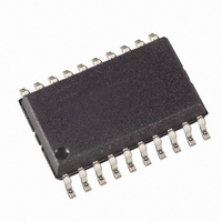
AT90PWM81-16SF Atmel, AT90PWM81-16SF Datasheet - Page 47

AT90PWM81-16SF
Manufacturer Part Number
AT90PWM81-16SF
Description
IC MCU AVR 8K FLASH ISP 20SOIC
Manufacturer
Atmel
Series
AVR® 90PWM Lightingr
Datasheet
1.AT90PWM81-16MN.pdf
(325 pages)
Specifications of AT90PWM81-16SF
Core Processor
AVR
Core Size
8-Bit
Speed
16MHz
Connectivity
SPI
Peripherals
Brown-out Detect/Reset, PWM, WDT
Number Of I /o
16
Program Memory Size
8KB (8K x 8)
Program Memory Type
FLASH
Eeprom Size
512 x 8
Ram Size
256 x 8
Voltage - Supply (vcc/vdd)
2.7 V ~ 5.5 V
Data Converters
A/D 8x10b; D/A 1x10b
Oscillator Type
Internal
Operating Temperature
-40°C ~ 105°C
Package / Case
20-SOIC (7.5mm Width)
For Use With
ATSTK600-SOIC - STK600 SOCKET/ADAPTER FOR SOIC
Lead Free Status / RoHS Status
Lead free / RoHS Compliant
Available stocks
Company
Part Number
Manufacturer
Quantity
Price
Company:
Part Number:
AT90PWM81-16SF
Manufacturer:
Atmel
Quantity:
2 428
- Current page: 47 of 325
- Download datasheet (6Mb)
6.7.7
6.8
6.8.1
6.8.2
7734P–AVR–08/10
Register description
On-chip Debug System
Sleep Mode Control Register – SMCR
Power Reduction Register - PRR
For analog input pins, the digital input buffer should be disabled at all times. An analog signal level close
to V
disabled by writing to the Digital Input Disable Registers (DIDR1 and DIDR0). Refer to “Digital Input
Disable Register 1– DIDR1” and “Digital Input Disable Register 0 – DIDR0” on
for details.
If the On-chip debug system is enabled by OCDEN Fuse and the chip enter sleep mode, the main clock
source is enabled, and hence, always consumes power. In the deeper sleep modes, this will contribute sig-
nificantly to the total current consumption.
The Sleep Mode Control Register contains control bits for power management.
• Bits 3..1 – SM2..0: Sleep Mode Select Bits 2, 1, and 0
These bits select between the five available sleep modes as shown in
Table 6-2.
Note:
• Bit 1 – SE: Sleep Enable
The SE bit must be written to logic one to make the MCU enter the sleep mode when the SLEEP instruc-
tion is executed. To avoid the MCU entering the sleep mode unless it is the programmer’s purpose, it is
recommended to write the Sleep Enable (SE) bit to one just before the execution of the SLEEP instruction
and to clear it immediately after waking up.
Bit
Read/Write
Initial Value
Bit
Read/Write
Initial Value
CC
SM2
/2 on an input pin can cause significant current even in active mode. Digital input buffers can be
0
0
0
0
1
1
1
1
1. Standby mode is only recommended for use with external crystals or resonators.
7
PRPSC2
R/W
0
7
–
R
0
Sleep Mode Select
SM1
-
6
R
0
0
0
1
1
0
0
1
1
6
–
R
0
5
PRPSCR
R/W
0
5
–
R
0
SM0
0
1
0
1
0
1
0
1
4
PRTIM1
R/W
0
4
–
R
0
Sleep Mode
Idle
ADC Noise Reduction
Power-down
Reserved
Reserved
Reserved
Standby
Reserved
3
-
R
0
3
SM2
R/W
0
(1)
2
PRSPI
R/W
0
2
SM1
R/W
0
Table
1
SM0
R/W
0
1
-
R
0
6-2.
AT90PWM81
page 202
0
SE
R/W
0
0
PRADC
R/W
0
and
SMCR
page 221
PRR
47
Related parts for AT90PWM81-16SF
Image
Part Number
Description
Manufacturer
Datasheet
Request
R

Part Number:
Description:
Manufacturer:
Atmel Corporation
Datasheet:

Part Number:
Description:
IC MCU AVR 8K FLASH ISP 20SOIC
Manufacturer:
Atmel
Datasheet:

Part Number:
Description:
IC MCU AVR 8K FLASH ISP 32QFN
Manufacturer:
Atmel
Datasheet:

Part Number:
Description:
IC MCU AVR 8K FLASH ISP 32QFN
Manufacturer:
Atmel
Datasheet:

Part Number:
Description:
8-bit Avr Microcontroller With 8k Bytes In- System Programmable Flash
Manufacturer:
ATMEL Corporation
Datasheet:

Part Number:
Description:
DEV KIT FOR AVR/AVR32
Manufacturer:
Atmel
Datasheet:

Part Number:
Description:
INTERVAL AND WIPE/WASH WIPER CONTROL IC WITH DELAY
Manufacturer:
ATMEL Corporation
Datasheet:

Part Number:
Description:
Low-Voltage Voice-Switched IC for Hands-Free Operation
Manufacturer:
ATMEL Corporation
Datasheet:

Part Number:
Description:
MONOLITHIC INTEGRATED FEATUREPHONE CIRCUIT
Manufacturer:
ATMEL Corporation
Datasheet:

Part Number:
Description:
AM-FM Receiver IC U4255BM-M
Manufacturer:
ATMEL Corporation
Datasheet:

Part Number:
Description:
Monolithic Integrated Feature Phone Circuit
Manufacturer:
ATMEL Corporation
Datasheet:

Part Number:
Description:
Multistandard Video-IF and Quasi Parallel Sound Processing
Manufacturer:
ATMEL Corporation
Datasheet:


