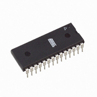
ATMEGA168PV-10PU Atmel, ATMEGA168PV-10PU Datasheet - Page 297

ATMEGA168PV-10PU
Manufacturer Part Number
ATMEGA168PV-10PU
Description
MCU AVR 16K FLASH 10MHZ 28-PDIP
Manufacturer
Atmel
Series
AVR® ATmegar
Specifications of ATMEGA168PV-10PU
Core Processor
AVR
Core Size
8-Bit
Speed
10MHz
Connectivity
I²C, SPI, UART/USART
Peripherals
Brown-out Detect/Reset, POR, PWM, WDT
Number Of I /o
23
Program Memory Size
16KB (8K x 16)
Program Memory Type
FLASH
Eeprom Size
512 x 8
Ram Size
1K x 8
Voltage - Supply (vcc/vdd)
1.8 V ~ 5.5 V
Data Converters
A/D 6x10b
Oscillator Type
Internal
Operating Temperature
-40°C ~ 85°C
Package / Case
28-DIP (0.300", 7.62mm)
Controller Family/series
AVR MEGA
No. Of I/o's
23
Eeprom Memory Size
512Byte
Ram Memory Size
1KB
Cpu Speed
10MHz
Rohs Compliant
Yes
For Use With
ATSTK600-TQFP32 - STK600 SOCKET/ADAPTER 32-TQFPATAVRDRAGON - KIT DRAGON 32KB FLASH MEM AVR
Lead Free Status / RoHS Status
Lead free / RoHS Compliant
- Current page: 297 of 420
- Download datasheet (9Mb)
27.7
27.7.1
8025L–AVR–7/10
Parallel Programming
Enter Programming Mode
Table 27-13. XA1 and XA0 Coding
Table 27-14. Command Byte Bit Coding
The following algorithm puts the device in Parallel (High-voltage) Programming mode:
1. Set Prog_enable pins listed in
2. Apply 4.5 - 5.5V between V
Ensure that V
3. Wait 20 - 60 µs, and apply 11.5 - 12.5V to RESET.
4. Keep the Prog_enable pins unchanged for at least 10µs after the High-voltage has been
5. Wait at least 300 µs before giving any parallel programming commands.
6. Exit Programming mode by power the device down or by bringing RESET pin to 0V.
If the rise time of the V
tive algorithm can be used.
1. Set Prog_enable pins listed in
2. Apply 4.5 - 5.5V between V
3. Monitor V
Command Byte
XA1
V
applied to ensure the Prog_enable Signature has been latched.
V
0
0
1
1
CC
CC
1000 0000
0100 0000
0010 0000
0001 0000
0001 0001
0000 1000
0000 0100
0000 0010
0000 0011
to 0V.
to 0V.
CC
CC
XA0
0
1
0
1
, and as soon as V
reaches at least 1.8V within the next 20 µs.
Action when XTAL1 is Pulsed
Load Flash or EEPROM Address (High or low address byte determined by BS1).
Load Data (High or Low data byte for Flash determined by BS1).
Load Command
No Action, Idle
Command Executed
Chip Erase
Write Fuse bits
Write Lock bits
Write Flash
Write EEPROM
Read Signature Bytes and Calibration byte
Read Fuse and Lock bits
Read Flash
Read EEPROM
CC
is unable to fulfill the requirements listed above, the following alterna-
CC
CC
Table 27-12 on page 296
and GND.
Table 27-12 on page 296
and GND.
CC
reaches 0.9 - 1.1V, apply 11.5 - 12.5V to RESET.
ATmega48P/88P/168P
to “0000”, RESET pin to 0V and
to “0000”, RESET pin to 0V and
297
Related parts for ATMEGA168PV-10PU
Image
Part Number
Description
Manufacturer
Datasheet
Request
R

Part Number:
Description:
Manufacturer:
Atmel Corporation
Datasheet:

Part Number:
Description:
MCU AVR 16K FLASH 20MHZ 32-TQFP
Manufacturer:
Atmel
Datasheet:

Part Number:
Description:
MCU AVR 16K FLASH 20MHZ 32-QFN
Manufacturer:
Atmel
Datasheet:

Part Number:
Description:
MCU AVR 16K FLASH 20MHZ 28-PDIP
Manufacturer:
Atmel
Datasheet:

Part Number:
Description:
MCU AVR 16KB FLASH 20MHZ 32TQFP
Manufacturer:
Atmel
Datasheet:

Part Number:
Description:
MCU AVR 16K FLASH 20MHZ 32-QFN
Manufacturer:
Atmel
Datasheet:

Part Number:
Description:
IC MCU AVR 16K FLASH 32TQFP
Manufacturer:
Atmel
Datasheet:

Part Number:
Description:
8-bit Microcontrollers - MCU Microcontroller
Manufacturer:
Atmel

Part Number:
Description:
Manufacturer:
Atmel Corporation
Datasheet:

Part Number:
Description:
Manufacturer:
Atmel Corporation
Datasheet:

Part Number:
Description:
Manufacturer:
ATMEL Corporation
Datasheet:


