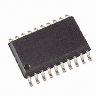
ATTINY861V-10SU Atmel, ATTINY861V-10SU Datasheet - Page 39

ATTINY861V-10SU
Manufacturer Part Number
ATTINY861V-10SU
Description
IC MCU AVR 8K FLASH 10MHZ 20SOIC
Manufacturer
Atmel
Series
AVR® ATtinyr
Specifications of ATTINY861V-10SU
Core Processor
AVR
Core Size
8-Bit
Speed
10MHz
Connectivity
USI
Peripherals
Brown-out Detect/Reset, POR, PWM, WDT
Number Of I /o
16
Program Memory Size
8KB (4K x 16)
Program Memory Type
FLASH
Eeprom Size
512 x 8
Ram Size
512 x 8
Voltage - Supply (vcc/vdd)
1.8 V ~ 5.5 V
Data Converters
A/D 11x10b
Oscillator Type
Internal
Operating Temperature
-40°C ~ 85°C
Package / Case
20-SOIC (7.5mm Width)
Processor Series
ATTINY8x
Core
AVR8
Data Bus Width
8 bit
Data Ram Size
512 B
Interface Type
2-Wire, SPI, USI
Maximum Clock Frequency
10 MHz
Number Of Programmable I/os
16
Number Of Timers
2
Maximum Operating Temperature
+ 85 C
Mounting Style
SMD/SMT
Minimum Operating Temperature
- 40 C
On-chip Adc
10 bit, 11 Channel
Package
20SOIC
Device Core
AVR
Family Name
ATtiny
Maximum Speed
10 MHz
Operating Supply Voltage
2.5|3.3|5 V
For Use With
ATSTK600-DIP40 - STK600 SOCKET/ADAPTER 40-PDIPATAVRBC100 - REF DESIGN KIT BATTERY CHARGER770-1007 - ISP 4PORT ATMEL AVR MCU SPI/JTAG770-1004 - ISP 4PORT FOR ATMEL AVR MCU SPI
Lead Free Status / RoHS Status
Lead free / RoHS Compliant
Available stocks
Company
Part Number
Manufacturer
Quantity
Price
Company:
Part Number:
ATTINY861V-10SU
Manufacturer:
Atmel
Quantity:
2 881
Company:
Part Number:
ATTINY861V-10SUR
Manufacturer:
Atmel
Quantity:
1 499
- Current page: 39 of 242
- Download datasheet (5Mb)
7.4
7.4.1
7.4.2
2588E–AVR–08/10
Register Description
MCUCR – MCU Control Register
PRR – Power Reduction Register
Refer to
able Register 1” on page 162
The MCU Control Register contains control bits for power management.
• Bit 5 – SE: Sleep Enable
The SE bit must be written to logic one to make the MCU enter the sleep mode when the SLEEP
instruction is executed. To avoid the MCU entering the sleep mode unless it is the programmer’s
purpose, it is recommended to write the Sleep Enable (SE) bit to one just before the execution of
the SLEEP instruction and to clear it immediately after waking up.
• Bits 4, 3 – SM1:0: Sleep Mode Select Bits 2:0
These bits select between the three available sleep modes as shown in
Table 7-2.
• Bit 2 – Res: Reserved Bit
This bit is reserved and will always read zero.
The Power Reduction Register provides a method to reduce power consumption by allowing
peripheral clock signals to be disabled.
• Bits 7, 6, 5, 4 – Res: Reserved Bits
These bits are reserved and will always read zero.
• Bit 3 – PRTIM1: Power Reduction Timer/Counter1
Writing a logic one to this bit shuts down the Timer/Counter1 module. When the Timer/Counter1
is enabled, operation will continue like before the shutdown.
Bit
0x35 (0x55)
Read/Write
Initial Value
Bit
0x36 (0x56)
Read/Write
Initial Value
SM1
0
0
1
1
“DIDR0 – Digital Input Disable Register 0” on page 162
7
–
R
0
Sleep Mode Select
7
–
R
0
6
PUD
R/W
0
6
-
R
0
SM0
0
1
0
1
for details.
5
SE
R/W
0
5
-
R
0
Sleep Mode
Idle
ADC Noise Reduction
Power-down
Standby
4
SM1
R/W
0
4
-
R
0
3
SM0
R/W
0
3
PRTIM1
R/W
0
2
—
R
0
2
PRTIM0
R/W
0
or
“DIDR1 – Digital Input Dis-
1
ISC01
R/W
0
1
PRUSI
R/W
0
Table
0
ISC00
R/W
0
7-2.
0
PRADC
R/W
0
MCUCR
PRR
39
Related parts for ATTINY861V-10SU
Image
Part Number
Description
Manufacturer
Datasheet
Request
R

Part Number:
Description:
Manufacturer:
Atmel Corporation
Datasheet:

Part Number:
Description:
Manufacturer:
Atmel Corporation
Datasheet:

Part Number:
Description:
IC MCU AVR 8K FLASH 20MHZ 32-QFN
Manufacturer:
Atmel
Datasheet:

Part Number:
Description:
IC MCU AVR 8K FLASH 20MHZ 20SOIC
Manufacturer:
Atmel
Datasheet:

Part Number:
Description:
MCU AVR 8K FLASH 15MHZ 32-QFN
Manufacturer:
Atmel
Datasheet:

Part Number:
Description:
MCU AVR 8K FLASH 15MHZ 20-SOIC
Manufacturer:
Atmel
Datasheet:

Part Number:
Description:
MCU AVR 8KB FLASH 15MHZ 32-VQFN
Manufacturer:
Atmel
Datasheet:

Part Number:
Description:
Microcontrollers (MCU) 8kB Flash 0.512kB EEPROM 16 I/O Pins
Manufacturer:
Atmel
Datasheet:

Part Number:
Description:
8-bit Microcontrollers - MCU 8KB FL 512B EE 512B SRAM 20MHZ IND 5V
Manufacturer:
Atmel

Part Number:
Description:
IC, MCU, 8BIT, 2K FLASH, 20SOIC
Manufacturer:
Atmel
Datasheet:


