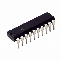
PIC16C782-I/P Microchip Technology, PIC16C782-I/P Datasheet - Page 65

PIC16C782-I/P
Manufacturer Part Number
PIC16C782-I/P
Description
IC MCU CMOS 8BIT 2K 20MHZ 20-DIP
Manufacturer
Microchip Technology
Series
PIC® 16Cr
Datasheets
1.PIC16C781-ISO.pdf
(186 pages)
2.PIC16C781-ISO.pdf
(8 pages)
3.PIC16C781-ISO.pdf
(8 pages)
Specifications of PIC16C782-I/P
Core Size
8-Bit
Program Memory Size
3.5KB (2K x 14)
Oscillator Type
Internal
Core Processor
PIC
Speed
20MHz
Peripherals
Brown-out Detect/Reset, POR, PWM, WDT
Number Of I /o
13
Program Memory Type
OTP
Ram Size
128 x 8
Voltage - Supply (vcc/vdd)
4 V ~ 5.5 V
Data Converters
A/D 8x8b; D/A 1x8b
Operating Temperature
-40°C ~ 85°C
Package / Case
20-DIP (0.300", 7.62mm)
Controller Family/series
PIC16C
No. Of I/o's
16
Ram Memory Size
128Byte
Cpu Speed
20MHz
No. Of Timers
2
No. Of
RoHS Compliant
Lead Free Status / RoHS Status
Lead free / RoHS Compliant
For Use With
DVA16XP202 - ADAPTER DEVICE PIC16C781/782DM163012 - BOARD DEMO PICDEM FOR 16C781/782AC164028 - MODULE SKT PROMATEII 20SOIC/DIP
Eeprom Size
-
Connectivity
-
Lead Free Status / RoHS Status
Lead free / RoHS Compliant
Other names
PIC16C782I/P
- Current page: 65 of 186
- Download datasheet (4Mb)
8.0
The PLVD module monitors the V
the microcontroller and signals the microcontroller
whenever V
acts as an ‘early warning’ of power-down, allowing the
microcontroller to finish any critical ‘housekeeping’
tasks prior to completing power-down.
Figure 8-1 demonstrates a potential application of the
PLVD module (typical battery operation). At time T
V
erence voltage. The PLVD voltage comparator then
sets the LVDIF bit (PIR<7>), indicating a low voltage
FIGURE 8-1:
8.1
The PLVD module is controlled via the LVDCON regis-
ter shown in Register 8-1.
To enable the module for testing, the LVDEN bit
(LVDCON<4>) must be set. This will enable the on-
board voltage reference and connect the resistor lad-
der between V
the module and disconnect the resistor ladder from
Vss.
DD
2001 Microchip Technology Inc.
supply voltage (V
PROGRAMMABLE LOW
VOLTAGE DETECT MODULE
(PLVD)
Control Register
DD
DD
drops below its trip voltage. The signal
and Vss. Clearing LVDEN will disable
V
V
A
B
A
TYPICAL LOW VOLTAGE DETECT APPLICATION
) has fallen below the PLVD ref-
DD
power supply of
Time
T
A
A
, the
Preliminary
T
B
condition. The time between T
to the microcontroller for completing a ‘graceful’ power-
down before V
Figure 8-2 is a simplified block diagram for the PLVD
module, showing the V
ter, and voltage comparator.
The trip voltage is set by programming the LVDL<3:0>
bit (LVDCON<3.0>). The voltages available are listed
in Register 8-1. Note that voltages below 2.5V and
above 4.75V are not available and should not be used.
The BGST bit (LVDCON<5>) is a status bit indicating
that the internal reference voltage bandgap has stabi-
lized. No test should be performed until this bit is set.
The low voltage output flag for the PLVD module is the
LVDIF bit (PIR1<6>).
Note:
Legend:
For low power applications, current drain
can be minimized by enabling the module
only during regular polled testing. When
not in use, the module is disabled by clear-
ing the LVDEN bit (LVDCON<4>), which
also powers down the resistor ladder
between V
V
V
A
B
DD
= PLVD trip point
= Minimum valid device
PIC16C781/782
operating voltage
falls below V
DD
DD
and Vss.
resistor ladder, control regis-
A
B
and T
.
DS41171A-page 63
B
is then available
Related parts for PIC16C782-I/P
Image
Part Number
Description
Manufacturer
Datasheet
Request
R

Part Number:
Description:
3.5KB Flash, 128B RAM, 18 I/O, CLC, CWG, DDS, 10-bit ADC 20 QFN 4x4mm TUBE
Manufacturer:
Microchip Technology
Datasheet:

Part Number:
Description:
3.5KB Flash, 128B RAM, 18 I/O, CLC, CWG, DDS, 10-bit ADC 20 PDIP .300in TUBE
Manufacturer:
Microchip Technology
Datasheet:

Part Number:
Description:
3.5KB Flash, 128B RAM, 18 I/O, CLC, CWG, DDS, 10-bit ADC 20 SOIC .300in TUBE
Manufacturer:
Microchip Technology
Datasheet:

Part Number:
Description:
3.5KB Flash, 128B RAM, 18 I/O, CLC, CWG, DDS, 10-bit ADC 20 SSOP .209in TUBE
Manufacturer:
Microchip Technology
Datasheet:

Part Number:
Description:
3.5KB Flash, 128B RAM, 18 I/O, CLC, CWG, DDS, 10-bit ADC 20 QFN 4x4mm TUBE
Manufacturer:
Microchip Technology
Datasheet:

Part Number:
Description:
3.5KB Flash, 128B RAM, 18 I/O, CLC, CWG, DDS, 10-bit ADC 20 PDIP .300in TUBE
Manufacturer:
Microchip Technology
Datasheet:

Part Number:
Description:
3.5KB Flash, 128B RAM, 18 I/O, CLC, CWG, DDS, 10-bit ADC 20 SOIC .300in TUBE
Manufacturer:
Microchip Technology
Datasheet:

Part Number:
Description:
3.5KB Flash, 128B RAM, 18 I/O, CLC, CWG, DDS, 10-bit ADC 20 SSOP .209in TUBE
Manufacturer:
Microchip Technology
Datasheet:

Part Number:
Description:
3.5KB Flash, 128B RAM, 18 I/O, CLC, CWG, DDS, 10-bit ADC 20 QFN 4x4mm T/R
Manufacturer:
Microchip Technology
Datasheet:

Part Number:
Description:
3.5KB Flash, 128B RAM, 18 I/O, CLC, CWG, DDS, 10-bit ADC 20 SOIC .300in T/R
Manufacturer:
Microchip Technology
Datasheet:

Part Number:
Description:
3.5KB Flash, 128B RAM, 18 I/O, CLC, CWG, DDS, 10-bit ADC 20 SSOP .209in T/R
Manufacturer:
Microchip Technology
Datasheet:

Part Number:
Description:
3.5KB Flash, 128B RAM, 18 I/O, CLC, CWG, DDS, 10-bit ADC 20 QFN 4x4mm TUBE
Manufacturer:
Microchip Technology
Datasheet:

Part Number:
Description:
3.5KB Flash, 128B RAM, 18 I/O, CLC, CWG, DDS, 10-bit ADC 20 PDIP .300in TUBE
Manufacturer:
Microchip Technology
Datasheet:

Part Number:
Description:
3.5KB Flash, 128B RAM, 18 I/O, CLC, CWG, DDS, 10-bit ADC 20 SOIC .300in TUBE
Manufacturer:
Microchip Technology
Datasheet:

Part Number:
Description:
3.5KB Flash, 128B RAM, 18 I/O, CLC, CWG, DDS, 10-bit ADC 20 SSOP .209in TUBE
Manufacturer:
Microchip Technology
Datasheet:


