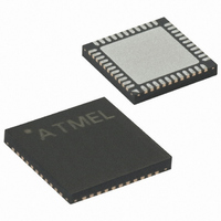
ATMEGA164PV-10MUR Atmel, ATMEGA164PV-10MUR Datasheet - Page 270

ATMEGA164PV-10MUR
Manufacturer Part Number
ATMEGA164PV-10MUR
Description
MCU AVR 16KB FLASH 10MHZ 44QFN
Manufacturer
Atmel
Series
AVR® ATmegar
Specifications of ATMEGA164PV-10MUR
Core Processor
AVR
Core Size
8-Bit
Speed
10MHz
Connectivity
I²C, SPI, UART/USART
Peripherals
Brown-out Detect/Reset, POR, PWM, WDT
Number Of I /o
32
Program Memory Size
16KB (8K x 16)
Program Memory Type
FLASH
Eeprom Size
512 x 8
Ram Size
1K x 8
Voltage - Supply (vcc/vdd)
1.8 V ~ 5.5 V
Data Converters
A/D 8x10b
Oscillator Type
Internal
Operating Temperature
-40°C ~ 85°C
Package / Case
44-VQFN Exposed Pad
For Use With
ATSTK600 - DEV KIT FOR AVR/AVR32
Lead Free Status / RoHS Status
Lead free / RoHS Compliant
- Current page: 270 of 439
- Download datasheet (10Mb)
8011O–AVR–07/10
The Boundary-scan logic is not included in the figures in the datasheet.
simple digital port pin as described in the section
details from
When no alternate port function is present, the Input Data - ID - corresponds to the PINxn Regis-
ter value (but ID has no synchronizer), Output Data corresponds to the PORT Register, Output
Control corresponds to the Data Direction - DD Register, and the Pull-up Enable - PUExn - cor-
responds to logic expression PUD · DDxn · PORTxn.
Digital alternate port functions are connected outside the dotted box in
scan chain read the actual pin value. For analog function, there is a direct connection from the
external pin to the analog circuit. There is no scan chain on the interface between the digital and
the analog circuitry, but some digital control signal to analog circuitry are turned off to avoid driv-
ing contention on the pads.
When JTAG IR contains EXTEST or SAMPLE_PRELOAD the clock is not sent out on the port
pins even if the CKOUT fuse is programmed. Even though the clock is output when the JTAG IR
contains SAMPLE_PRELOAD, the clock is not sampled by the boundary scan.
Figure 22-3. Boundary-scan Cell for Bi-directional Port Pin with Pull-up Function.
Pull-up Enable (PUE)
Output Control (OC)
Output Data (OD)
Input Data (ID)
Figure 22-3
replaces the dashed box in
0
1
From Last Cell
0
1
0
1
ShiftDR
ClockDR
D
D
FF1
FF0
To Next Cell
Q
Q
ATmega164P/324P/644P
”I/O-Ports” on page
UpdateDR
Figure
D
G
D
G
LD1
LD0
22-4.
Q
Q
0
1
0
1
0
1
EXTEST
Figure 22-4
72. The Boundary-scan
Figure 22-4
Vcc
to make the
shows a
270
Related parts for ATMEGA164PV-10MUR
Image
Part Number
Description
Manufacturer
Datasheet
Request
R

Part Number:
Description:
Manufacturer:
Atmel Corporation
Datasheet:

Part Number:
Description:
Manufacturer:
Atmel Corporation
Datasheet:

Part Number:
Description:
IC MCU AVR 16K FLASH 44-TQFP
Manufacturer:
Atmel
Datasheet:

Part Number:
Description:
IC MCU AVR 16K FLASH 44-QFN
Manufacturer:
Atmel
Datasheet:

Part Number:
Description:
MCU AVR 16K FLASH 20MHZ 44-TQFP
Manufacturer:
Atmel
Datasheet:

Part Number:
Description:
MCU AVR 16KB FLASH 15MHZ 44TQFP
Manufacturer:
Atmel
Datasheet:

Part Number:
Description:
IC MCU AVR 16K FLASH 40-DIP
Manufacturer:
Atmel
Datasheet:

Part Number:
Description:
MCU AVR 16KB FLASH 20MHZ 44-VQFN
Manufacturer:
Atmel
Datasheet:

Part Number:
Description:
MCU AVR 16KB FLASH 20MHZ 44TQFP
Manufacturer:
Atmel
Datasheet:

Part Number:
Description:
MCU AVR 16K FLASH 20MHZ 44-QFN
Manufacturer:
Atmel
Datasheet:

Part Number:
Description:
MCU AVR 16K FLASH 20MHZ 40-PDIP
Manufacturer:
Atmel
Datasheet:

Part Number:
Description:
MCU AVR 16KB FLASH 15MHZ 44TQFP
Manufacturer:
Atmel
Datasheet:


