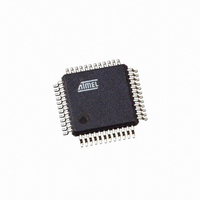
AT91SAM7S32B-AU-999 Atmel, AT91SAM7S32B-AU-999 Datasheet - Page 535

AT91SAM7S32B-AU-999
Manufacturer Part Number
AT91SAM7S32B-AU-999
Description
IC MCU ARM7 32KB FLASH 48LQFP
Manufacturer
Atmel
Series
AT91SAMr
Datasheet
1.AT91SAM7S16-MU.pdf
(779 pages)
Specifications of AT91SAM7S32B-AU-999
Core Processor
ARM7
Core Size
16/32-Bit
Speed
55MHz
Connectivity
I²C, SPI, SSC, UART/USART
Peripherals
Brown-out Detect/Reset, DMA, POR, PWM, WDT
Number Of I /o
21
Program Memory Size
32KB (32K x 8)
Program Memory Type
FLASH
Ram Size
8K x 8
Voltage - Supply (vcc/vdd)
1.65 V ~ 1.95 V
Data Converters
A/D 8x10b
Oscillator Type
Internal
Operating Temperature
-40°C ~ 85°C
Package / Case
48-LQFP
Processor Series
AT91SAMx
Core
ARM7TDMI
Data Bus Width
32 bit
Data Ram Size
8 KB
Interface Type
I2C, JTAG, SPI, USART
Maximum Clock Frequency
55 MHz
Number Of Programmable I/os
21
Operating Supply Voltage
3.3 V
Maximum Operating Temperature
+ 85 C
Mounting Style
SMD/SMT
3rd Party Development Tools
JTRACE-ARM-2M, KSK-AT91SAM7S-PL, MDK-ARM, RL-ARM, ULINK2
Development Tools By Supplier
AT91SAM-ICE, AT91-ISP, AT91SAM7S-EK
Minimum Operating Temperature
- 40 C
For Use With
AT91SAM-ICE - EMULATOR FOR AT91 ARM7/ARM9AT91SAM7S-EK - KIT EVAL FOR ARM AT91SAM7S
Lead Free Status / RoHS Status
Lead free / RoHS Compliant
Eeprom Size
-
Lead Free Status / Rohs Status
Details
Available stocks
Company
Part Number
Manufacturer
Quantity
Price
- Current page: 535 of 779
- Download datasheet (11Mb)
36. Analog-to-Digital Converter (ADC)
36.1
36.2
Figure 36-1. Analog-to-Digital Converter Block Diagram
6175K–ATARM–30-Aug-10
Overview
Block Diagram
Analog Inputs
with I/O lines
Multiplexed
Dedicated
Analog
Inputs
ADVREF
ADTRG
VDDIN
AD-
AD-
AD-
AD-
AD-
AD-
GND
The ADC is based on a Successive Approximation Register (SAR) 10-bit Analog-to-Digital Con-
verter (ADC). It also integrates an 8-to-1 analog multiplexer, making possible the analog-to-
digital conversions of 8 analog lines. The conversions extend from 0V to ADVREF.
The ADC supports an 8-bit or 10-bit resolution mode, and conversion results are reported in a
common register for all channels, as well as in a channel-dedicated register. Software trigger,
external trigger on rising edge of the ADTRG pin or internal triggers from Timer Counter out-
put(s) are configurable.
The ADC also integrates a Sleep Mode and a conversion sequencer and connects with a PDC
channel. These features reduce both power consumption and processor intervention.
Finally, the user can configure ADC timings, such as Startup Time and Sample & Hold Time.
PIO
Selection
Channels
Trigger
Counter
Timer
Analog-to-Digital
Approximation
ADC cell
Successive
Converter
Register
ADC Controller
AT91SAM7S Series Preliminary
Interface
Control
PMC
Logic
User
MCK
ADC Interrupt
PDC
AIC
Peripheral Bridge
ASB
APB
535
Related parts for AT91SAM7S32B-AU-999
Image
Part Number
Description
Manufacturer
Datasheet
Request
R

Part Number:
Description:
Manufacturer:
ATMEL Corporation
Datasheet:

Part Number:
Description:
IC ARM7 MCU 32BIT 32K 48LQFP
Manufacturer:
Atmel
Datasheet:

Part Number:
Description:
AT91 ARM Thumb-based Microcontrollers
Manufacturer:
ATMEL [ATMEL Corporation]
Datasheet:

Part Number:
Description:
IC ARM7 MCU FLASH 32K 48QFN
Manufacturer:
Atmel
Datasheet:

Part Number:
Description:
IC MCU ARM7 32KB FLASH 48LQFP
Manufacturer:
Atmel
Datasheet:

Part Number:
Description:
IC MCU ARM7 32KB FLASH 48-VQFN
Manufacturer:
Atmel
Datasheet:

Part Number:
Description:
DEV KIT FOR AVR/AVR32
Manufacturer:
Atmel
Datasheet:

Part Number:
Description:
INTERVAL AND WIPE/WASH WIPER CONTROL IC WITH DELAY
Manufacturer:
ATMEL Corporation
Datasheet:

Part Number:
Description:
Low-Voltage Voice-Switched IC for Hands-Free Operation
Manufacturer:
ATMEL Corporation
Datasheet:

Part Number:
Description:
MONOLITHIC INTEGRATED FEATUREPHONE CIRCUIT
Manufacturer:
ATMEL Corporation
Datasheet:

Part Number:
Description:
AM-FM Receiver IC U4255BM-M
Manufacturer:
ATMEL Corporation
Datasheet:

Part Number:
Description:
Monolithic Integrated Feature Phone Circuit
Manufacturer:
ATMEL Corporation
Datasheet:

Part Number:
Description:
Multistandard Video-IF and Quasi Parallel Sound Processing
Manufacturer:
ATMEL Corporation
Datasheet:


