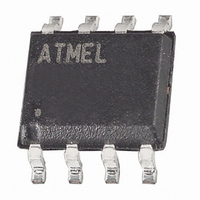
ATTINY85-15ST1 Atmel, ATTINY85-15ST1 Datasheet - Page 123

ATTINY85-15ST1
Manufacturer Part Number
ATTINY85-15ST1
Description
MCU AVR 8K FLASH 15MHZ 8-SOIC
Manufacturer
Atmel
Series
AVR® ATtinyr
Datasheet
1.ATTINY25-15MZ.pdf
(196 pages)
Specifications of ATTINY85-15ST1
Package / Case
8-SOIC (3.9mm Width)
Voltage - Supply (vcc/vdd)
2.7 V ~ 5.5 V
Operating Temperature
-40°C ~ 105°C
Speed
16MHz
Number Of I /o
6
Eeprom Size
512 x 8
Core Processor
AVR
Program Memory Type
FLASH
Ram Size
512 x 8
Program Memory Size
8KB (8K x 8)
Data Converters
A/D 4x10b
Oscillator Type
Internal
Peripherals
Brown-out Detect/Reset, POR, PWM, WDT
Connectivity
USI
Core Size
8-Bit
Lead Free Status / RoHS Status
Lead free / RoHS Compliant
- Current page: 123 of 196
- Download datasheet (4Mb)
18.7.5
7598H–AVR–07/09
ADC Multiplexer Selection Register – ADMUX
The values described in Table 51 are typical values. However, due to the process variation the
temperature sensor output voltage varies from one chip to another. To be capable of achieving
more accurate results the temperature measurement can be calibrated in the application soft-
ware. The software calibration requires that a calibration value is measured and stored in a
register or EEPROM for each chip, as a part of the production test. The sofware calibration can
be done utilizing the formula:
where V
is the temperature sensor offset value determined and stored into EEPROM as a part of produc-
tion test.
• Bit 7..6,4 – REFS2..REFS0: Voltage Reference Selection Bits
These bits select the voltage reference (V
are changed during a conversion, the change will not go in effect until this conversion is
complete (ADIF in ADCSR is set). Whenever these bits are changed, the next conversion will
take 25 ADC clock cycles. If active channels are used, using V
than (V
Table 18-3.
1.
• Bit 5 – ADLAR: ADC Left Adjust Result
The ADLAR bit affects the presentation of the ADC conversion result in the ADC Data Register.
Write one to ADLAR to left adjust the result. Otherwise, the result is right adjusted. Changing the
ADLAR bit will affect the ADC Data Register immediately, regardless of any ongoing conver-
sions. For a comple te description of this bit, see
on page
Temperature
Bit
Read/Write
Initial Value
REFS2
0
0
0
0
1
1
CC
TEMP
The device requires a supply voltage of 3V in order to generate 2.56V reference voltage.
126.
- 1V) as a voltage reference is not recommended, as this will affect the ADC accuracy.
is the ADC reading of the temperature sensor signal, k is a fixed coefficient and T
REFS1
=
Voltage Reference Selections for ADC
REFS1
0
0
1
1
1
1
k
R
7
0
V
TEMP
REFS0
REFS0
R/W
6
0
0
1
0
1
0
1
+
T
OS
ADLAR
R/W
Voltage Reference (V
V
External Voltage Reference at PB0 (AREF) pin, Internal Voltage
Reference turned off.
Internal 1.1V Voltage Reference without external bypass capacitor,
disconnected from PB0 (AREF).
Internal 1.1V Voltage Reference with external bypass capacitor at
PB0 (AREF) pin.
Internal 2.56V Voltage Reference without external bypass
capacitor, disconnected from PB0 (AREF).
Internal 2.56V Voltage Reference with external bypass capacitor at
PB0 (AREF) pin.
5
0
CC
used as Voltage Reference, disconnected from PB0 (AREF).
REF
REFS2
R
4
0
) for the ADC, as shown in
(1)
“The ADC Data Register – ADCL and ADCH”
MUX3
R
3
0
REF
) Selection
MUX2
R
2
0
CC
ATtiny25/45/85
or an external AREF higher
MUX1
R/W
1
0
Table
(1)
18-3. If these bits
MUX0
R/W
0
0
ADMUX
123
OS
Related parts for ATTINY85-15ST1
Image
Part Number
Description
Manufacturer
Datasheet
Request
R

Part Number:
Description:
Manufacturer:
Atmel Corporation
Datasheet:

Part Number:
Description:
Manufacturer:
Atmel Corporation
Datasheet:

Part Number:
Description:
IC AVR MCU 8K 20MHZ 8SOIC
Manufacturer:
Atmel
Datasheet:

Part Number:
Description:
IC MCU AVR 8K FLASH 20MHZ 20-QFN
Manufacturer:
Atmel
Datasheet:

Part Number:
Description:
IC AVR MCU 8K 20MHZ 8DIP
Manufacturer:
Atmel
Datasheet:

Part Number:
Description:
MCU AVR 8KB FLASH 20MHZ 8SOIC
Manufacturer:
Atmel
Datasheet:

Part Number:
Description:
IC MCU AVR 8KB FLASH 20MHZ 8SOIC
Manufacturer:
Atmel
Datasheet:

Part Number:
Description:
MCU AVR 8KB FLASH 20MHZ 20QFN
Manufacturer:
Atmel
Datasheet:

Part Number:
Description:
IC AVR MCU 8K 20MHZ 8DIP
Manufacturer:
Atmel
Datasheet:

Part Number:
Description:
IC AVR MCU 8K 20MHZ 8SOIC
Manufacturer:
Atmel
Datasheet:


