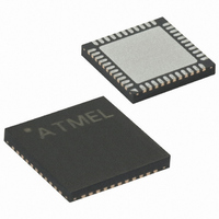
ATMEGA8535L-8MU Atmel, ATMEGA8535L-8MU Datasheet - Page 8

ATMEGA8535L-8MU
Manufacturer Part Number
ATMEGA8535L-8MU
Description
IC AVR MCU 8K 8MHZ 3V 44-QFN
Manufacturer
Atmel
Series
AVR® ATmegar
Specifications of ATMEGA8535L-8MU
Core Processor
AVR
Core Size
8-Bit
Speed
8MHz
Connectivity
I²C, SPI, UART/USART
Peripherals
Brown-out Detect/Reset, POR, PWM, WDT
Number Of I /o
32
Program Memory Size
8KB (4K x 16)
Program Memory Type
FLASH
Eeprom Size
512 x 8
Ram Size
512 x 8
Voltage - Supply (vcc/vdd)
2.7 V ~ 5.5 V
Data Converters
A/D 8x10b
Oscillator Type
Internal
Operating Temperature
-40°C ~ 85°C
Package / Case
44-VQFN Exposed Pad
Processor Series
ATMEGA8x
Core
AVR8
Data Bus Width
8 bit
Data Ram Size
512 B
Interface Type
SPI, TWI, UART
Maximum Clock Frequency
8 MHz
Number Of Programmable I/os
32
Number Of Timers
3
Operating Supply Voltage
2.7 V to 5.5 V
Maximum Operating Temperature
+ 85 C
Mounting Style
SMD/SMT
3rd Party Development Tools
EWAVR, EWAVR-BL
Minimum Operating Temperature
- 40 C
On-chip Adc
10 bit, 8 Channel
Package
44MLF EP
Device Core
AVR
Family Name
ATmega
Maximum Speed
8 MHz
For Use With
ATSTK600-DIP40 - STK600 SOCKET/ADAPTER 40-PDIP770-1007 - ISP 4PORT ATMEL AVR MCU SPI/JTAGATAVRISP2 - PROGRAMMER AVR IN SYSTEMATSTK500 - PROGRAMMER AVR STARTER KIT
Lead Free Status / RoHS Status
Lead free / RoHS Compliant
Available stocks
Company
Part Number
Manufacturer
Quantity
Price
Part Number:
ATMEGA8535L-8MU
Manufacturer:
ATMEL/爱特梅尔
Quantity:
20 000
- Current page: 8 of 321
- Download datasheet (3Mb)
AVR CPU Core
Introduction
Architectural Overview
8
ATmega8535(L)
This section discusses the AVR core architecture in general. The main function of the
CPU core is to ensure correct program execution. The CPU must therefore be able to
access memories, perform calculations, control peripherals, and handle interrupts.
Figure 3. Block Diagram of the AVR MCU Architecture
In order to maximize performance and parallelism, the AVR uses a Harvard architecture
– with separate memories and buses for program and data. Instructions in the program
memory are executed with a single level pipelining. While one instruction is being exe-
cuted, the next instruction is pre-fetched from the program memory. This concept
enables instructions to be executed in every clock cycle. The program memory is In-
System Re-Programmable Flash memory.
The fast-access Register File contains 32 x 8-bit general purpose working registers with
a single clock cycle access time. This allows single-cycle Arithmetic Logic Unit (ALU)
operation. In a typical ALU operation, two operands are output from the Register File,
the operation is executed, and the result is stored back in the Register File – in one
clock cycle.
Control Lines
Instruction
Instruction
Program
Memory
Register
Decoder
Flash
Program
Counter
and Control
EEPROM
Registrers
I/O Lines
Purpose
General
SRAM
8-bit Data Bus
Status
32 x 8
Data
ALU
I/O Module 2
Comparator
I/O Module1
I/O Module n
2502K–AVR–10/06
Watchdog
Interrupt
Timer
Analog
Unit
Unit
SPI
Related parts for ATMEGA8535L-8MU
Image
Part Number
Description
Manufacturer
Datasheet
Request
R

Part Number:
Description:
IC AVR MCU 2.4GHZ XCEIVER 64QFN
Manufacturer:
Atmel
Datasheet:

Part Number:
Description:
Manufacturer:
Atmel
Datasheet:

Part Number:
Description:
MCU ATMEGA644/AT86RF230 40-DIP
Manufacturer:
Atmel
Datasheet:

Part Number:
Description:
BUNDLE ATMEGA644P/AT86RF230 QFN
Manufacturer:
Atmel
Datasheet:

Part Number:
Description:
BUNDLE ATMEGA644P/AT86RF230 TQFP
Manufacturer:
Atmel
Datasheet:

Part Number:
Description:
MCU ATMEGA1281/AT86RF230 64-TQFP
Manufacturer:
Atmel
Datasheet:

Part Number:
Description:
MCU ATMEGA1280/AT86RF230 100TQFP
Manufacturer:
Atmel
Datasheet:

Part Number:
Description:
BUNDLE ATMEGA1280/AT86RF100-TQFP
Manufacturer:
Atmel
Datasheet:

Part Number:
Description:
BUNDLE ATMEGA2560V/AT86RF230-ZU
Manufacturer:
Atmel
Datasheet:

Part Number:
Description:
MCU ATMEGA2561/AT86RF230 64-TQFP
Manufacturer:
Atmel
Datasheet:

Part Number:
Description:
INTERVAL AND WIPE/WASH WIPER CONTROL IC WITH DELAY
Manufacturer:
ATMEL Corporation
Datasheet:

Part Number:
Description:
Low-Voltage Voice-Switched IC for Hands-Free Operation
Manufacturer:
ATMEL Corporation
Datasheet:

Part Number:
Description:
MONOLITHIC INTEGRATED FEATUREPHONE CIRCUIT
Manufacturer:
ATMEL Corporation
Datasheet:

Part Number:
Description:
AM-FM Receiver IC U4255BM-M
Manufacturer:
ATMEL Corporation
Datasheet:


