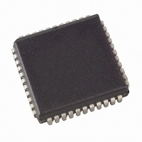
AT89S8253-24JU Atmel, AT89S8253-24JU Datasheet - Page 27

AT89S8253-24JU
Manufacturer Part Number
AT89S8253-24JU
Description
IC MCU 12K FLASH 24MHZ 44-PLCC
Manufacturer
Atmel
Series
89Sr
Datasheet
1.AT89S8253-24PU.pdf
(60 pages)
Specifications of AT89S8253-24JU
Core Processor
8051
Core Size
8-Bit
Speed
24MHz
Connectivity
SPI, UART/USART
Peripherals
POR, WDT
Number Of I /o
32
Program Memory Size
12KB (12K x 8)
Program Memory Type
FLASH
Eeprom Size
2K x 8
Ram Size
256 x 8
Voltage - Supply (vcc/vdd)
2.7 V ~ 5.5 V
Oscillator Type
Internal
Operating Temperature
-40°C ~ 85°C
Package / Case
44-PLCC
Processor Series
AT89x
Core
8051
Data Bus Width
8 bit
Data Ram Size
256 B
Interface Type
SPI/UART
Maximum Clock Frequency
24 MHz
Number Of Programmable I/os
32
Number Of Timers
3
Operating Supply Voltage
2.7 V to 5.5 V
Maximum Operating Temperature
+ 85 C
Mounting Style
SMD/SMT
3rd Party Development Tools
PK51, CA51, A51, ULINK2
Development Tools By Supplier
AT89ISP
Minimum Operating Temperature
- 40 C
Lead Free Status / RoHS Status
Lead free / RoHS Compliant
Data Converters
-
Lead Free Status / Rohs Status
Lead free / RoHS Compliant
Available stocks
Company
Part Number
Manufacturer
Quantity
Price
Company:
Part Number:
AT89S8253-24JU
Manufacturer:
LITTLEFUSE
Quantity:
4 500
Company:
Part Number:
AT89S8253-24JU
Manufacturer:
ATMEL
Quantity:
6
Company:
Part Number:
AT89S8253-24JU
Manufacturer:
ATMEL
Quantity:
5 530
Company:
Part Number:
AT89S8253-24JU
Manufacturer:
ATM
Quantity:
3 290
Company:
Part Number:
AT89S8253-24JU
Manufacturer:
ATMEL
Quantity:
44 616
Part Number:
AT89S8253-24JU
Manufacturer:
ATMEL/爱特梅尔
Quantity:
20 000
3286P–MICRO–3/10
Figure 14-3. SPI Shift Register Diagram
The CPHA (Clock PHAse), CPOL (Clock POLarity), and SPR (Serial Peripheral clock Rate =
baud rate) bits in SPCR control the shape and rate of SCK. The two SPR bits provide four possi-
ble clock rates when the SPI is in master mode. In slave mode, the SPI will operate at the rate of
the incoming SCK as long as it does not exceed the maximum bit rate. There are also four pos-
sible combinations of SCK phase and polarity with respect to the serial data. CPHA and CPOL
determine which format is used for transmission. The SPI data transfer formats are shown in
Figure 14-4
CPOL, and SPR should be set up before the interface is enabled, and the master device should
be enabled before the slave device(s).
Table 14-4.
Symbol
t
t
t
t
t
t
t
t
t
t
Transmit
CLCL
SCK
SHSL
SLSH
SR
SF
SIS
SIH
SOH
SOV
Serial In
Byte
and
8
SPI Master Characteristics
Parameter
Oscillator Period
Serial Clock Cycle Time
Clock High Time
Clock Low Time
Rise Time
Fall Time
Serial Input Setup Time
Serial Input Hold Time
Serial Output Hold Time
Serial Output Valid Time
Figure
MUX
8
2:1
14-5. To prevent glitches on SCK from disrupting the interface, CPHA,
8
Parallel Master
Serial Master
(Write Buffer)
D
CLK
D
CLK
LATCH
LATCH
Q
Q
7
t
t
SCK
SCK
4t
41.6
Min
/2 - 25
/2 - 25
10
10
CLCL
MUX
2:1
8
Parallel Slave
Serial Slave
Max
(Read Buffer)
25
35
25
10
D
CLK
D
CLK
AT89S8253
LATCH
LATCH
Q
Q
8
Units
Serial Out
Receive
ns
ns
ns
ns
ns
ns
ns
ns
ns
ns
Byte
27


