PIC18F27J13-I/ML Microchip Technology, PIC18F27J13-I/ML Datasheet - Page 109
PIC18F27J13-I/ML
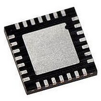
Manufacturer Part Number
PIC18F27J13-I/ML
Description
IC PIC MCU 128KB FLASH 28QFN
Manufacturer
Microchip Technology
Series
PIC® XLP™ 18Fr
Datasheets
1.PIC18LF24J10-ISS.pdf
(32 pages)
2.PIC18F26J13-ISS.pdf
(496 pages)
3.PIC18F26J13-ISS.pdf
(558 pages)
4.PIC18F26J13-ISS.pdf
(12 pages)
Specifications of PIC18F27J13-I/ML
Core Size
8-Bit
Program Memory Size
128KB (64K x 16)
Core Processor
PIC
Speed
48MHz
Connectivity
I²C, LIN, SPI, UART/USART
Peripherals
Brown-out Detect/Reset, POR, PWM, WDT
Number Of I /o
22
Program Memory Type
FLASH
Ram Size
3.8K x 8
Voltage - Supply (vcc/vdd)
2.15 V ~ 3.6 V
Data Converters
A/D 10x10b/12b
Oscillator Type
Internal
Operating Temperature
-40°C ~ 85°C
Package / Case
*
Controller Family/series
PIC18
Cpu Speed
48MHz
Digital Ic Case Style
QFN
Supply Voltage Range
1.8V To 5.5V
Embedded Interface Type
I2C, SPI, USART
Rohs Compliant
Yes
Processor Series
PIC18F
Core
PIC
Data Bus Width
8 bit
Data Ram Size
4 KB
Interface Type
I2C, SPI, EUSART
Maximum Clock Frequency
48 MHz
Number Of Programmable I/os
19
Number Of Timers
8
Operating Supply Voltage
2 V to 3.6 V
Maximum Operating Temperature
+ 85 C
Mounting Style
SMD/SMT
3rd Party Development Tools
52715-96, 52716-328, 52717-734, 52712-325, EWPIC18
Development Tools By Supplier
DM164128, DM180021, DM183026-2, DV164131, MA180030, DM183022, DM183032, DV164136, MA180024
Minimum Operating Temperature
- 40 C
On-chip Adc
12 bit, 10 Channel
Lead Free Status / RoHS Status
Lead free / RoHS Compliant
For Use With
MA180030 - BOARD DEMO PIC18F47J13 FS USBMA180029 - BOARD DEMO PIC18F47J53 FS USB
Eeprom Size
-
Lead Free Status / Rohs Status
Details
Available stocks
Company
Part Number
Manufacturer
Quantity
Price
Company:

Part Number:
PIC18F27J13-I/ML
Manufacturer:
MICROCHIP
Quantity:
4 000


REGISTER 7-1:
2010 Microchip Technology Inc.
bit 7
Legend:
R = Readable bit
-n = Value at POR
bit 7-6
bit 5
bit 4
bit 3
bit 2
bit 1
bit 0
U-0
—
Unimplemented: Read as ‘0’
WPROG: One Word-Wide Program bit
1 = Program 2 bytes on the next WR command
0 = Program 64 bytes on the next WR command
FREE: Flash Erase Enable bit
1 = Perform an erase operation on the next WR command (cleared by hardware after completion of erase)
0 = Perform write-only
WRERR: Flash Program Error Flag bit
1 = A write operation is prematurely terminated (any Reset during self-timed programming in normal
0 = The write operation completed
WREN: Flash Program Write Enable bit
1 = Allows write cycles to Flash program memory
0 = Inhibits write cycles to Flash program memory
WR: Write-Control bit
1 = Initiates a program memory erase cycle or write cycle
0 = Write cycle is complete
Unimplemented: Read as ‘0’
U-0
operation or an improper write attempt)
(The operation is self-timed and the bit is cleared by hardware once the write is complete. The WR
bit can only be set (not cleared) in software.)
—
EECON1: EEPROM CONTROL REGISTER 1 (ACCESS FA6h)
S = Settable bit (cannot be cleared in software)
W = Writable bit
‘1’ = Bit is set
WPROG
R/W-0
Preliminary
R/W-0
FREE
PIC18F47J13 FAMILY
U = Unimplemented bit, read as ‘0’
‘0’ = Bit is cleared
WRERR
R/W-x
WREN
R/W-0
x = Bit is unknown
R/S-0
WR
DS39974A-page 109
U-0
—
bit 0
Related parts for PIC18F27J13-I/ML
Image
Part Number
Description
Manufacturer
Datasheet
Request
R

Part Number:
Description:
Manufacturer:
Microchip Technology Inc.
Datasheet:
Part Number:
Description:
Manufacturer:
Microchip Technology Inc.
Datasheet:
Part Number:
Description:
Manufacturer:
Microchip Technology Inc.
Datasheet:
Part Number:
Description:
Manufacturer:
Microchip Technology Inc.
Datasheet:
Part Number:
Description:
Manufacturer:
Microchip Technology Inc.
Datasheet:
Part Number:
Description:
Manufacturer:
Microchip Technology Inc.
Datasheet:
Part Number:
Description:
Manufacturer:
Microchip Technology Inc.
Datasheet:
Part Number:
Description:
Manufacturer:
Microchip Technology Inc.
Datasheet: