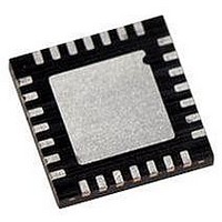
PIC18F27J13-I/ML Microchip Technology, PIC18F27J13-I/ML Datasheet - Page 7

PIC18F27J13-I/ML
Manufacturer Part Number
PIC18F27J13-I/ML
Description
IC PIC MCU 128KB FLASH 28QFN
Manufacturer
Microchip Technology
Series
PIC® XLP™ 18Fr
Datasheets
1.PIC18LF24J10-ISS.pdf
(32 pages)
2.PIC18F26J13-ISS.pdf
(496 pages)
3.PIC18F26J13-ISS.pdf
(558 pages)
4.PIC18F26J13-ISS.pdf
(12 pages)
Specifications of PIC18F27J13-I/ML
Core Size
8-Bit
Program Memory Size
128KB (64K x 16)
Core Processor
PIC
Speed
48MHz
Connectivity
I²C, LIN, SPI, UART/USART
Peripherals
Brown-out Detect/Reset, POR, PWM, WDT
Number Of I /o
22
Program Memory Type
FLASH
Ram Size
3.8K x 8
Voltage - Supply (vcc/vdd)
2.15 V ~ 3.6 V
Data Converters
A/D 10x10b/12b
Oscillator Type
Internal
Operating Temperature
-40°C ~ 85°C
Package / Case
*
Controller Family/series
PIC18
Cpu Speed
48MHz
Digital Ic Case Style
QFN
Supply Voltage Range
1.8V To 5.5V
Embedded Interface Type
I2C, SPI, USART
Rohs Compliant
Yes
Processor Series
PIC18F
Core
PIC
Data Bus Width
8 bit
Data Ram Size
4 KB
Interface Type
I2C, SPI, EUSART
Maximum Clock Frequency
48 MHz
Number Of Programmable I/os
19
Number Of Timers
8
Operating Supply Voltage
2 V to 3.6 V
Maximum Operating Temperature
+ 85 C
Mounting Style
SMD/SMT
3rd Party Development Tools
52715-96, 52716-328, 52717-734, 52712-325, EWPIC18
Development Tools By Supplier
DM164128, DM180021, DM183026-2, DV164131, MA180030, DM183022, DM183032, DV164136, MA180024
Minimum Operating Temperature
- 40 C
On-chip Adc
12 bit, 10 Channel
Lead Free Status / RoHS Status
Lead free / RoHS Compliant
For Use With
MA180030 - BOARD DEMO PIC18F47J13 FS USBMA180029 - BOARD DEMO PIC18F47J53 FS USB
Eeprom Size
-
Lead Free Status / Rohs Status
Details
Available stocks
Company
Part Number
Manufacturer
Quantity
Price
Company:
Part Number:
PIC18F27J13-I/ML
Manufacturer:
MICROCHIP
Quantity:
4 000
2.3
Figure 2-5 shows the high-level overview of the
programming process. First, a Bulk Erase is performed.
Next, the code memory is programmed. Since the only
nonvolatile Configuration Words are within the code
memory space, they too are programmed as if they
were code. Code memory (including the Configuration
Words) is then verified to ensure that programming was
successful.
FIGURE 2-5:
FIGURE 2-6:
© 2009 Microchip Technology Inc.
MCLR
V
PGD
PGC
DD
Overview of the Programming
Process
Program Memory
Verify Program
Enter ICSP™
Perform Bulk
P13
HIGH-LEVEL
PROGRAMMING FLOW
ENTERING PROGRAM/VERIFY MODE
Exit ICSP
Erase
Done
Done
Start
P1
P19
V
b31
PIC18F2XJXX/4XJXX FAMILY
IH
0
b30
1
Program/Verify Entry Code = 4D434850h
b29
0
b28
P2B
0
P2A
b27
2.4
Entry into ICSP modes for PIC18F2XJXX/4XJXX family
devices is somewhat different than previous PIC18
devices. As shown in Figure 2-6, entering ICSP
Program/Verify mode requires three steps:
1.
2.
3.
The programming voltage applied to MCLR is V
essentially, V
for holding at V
least P19 must elapse before presenting the key
sequence on PGD.
The key sequence is a specific 32-bit pattern,
‘0100 1101 0100 0011 0100 1000 0101 0000’
(more easily remembered as 4D434850h in hexa-
decimal). The device will enter Program/Verify mode
only if the sequence is valid. The Most Significant bit of
the most significant nibble must be shifted in first.
Once the key sequence is complete, V
applied to MCLR and held at that level for as long as
Program/Verify mode is to be maintained. An interval of
at least time, P20 and P12, must elapse before present-
ing data on PGD. Signals appearing on PGD before P12
has elapsed may not be interpreted as valid.
On successful entry, the program memory can be
accessed and programmed in serial fashion. While in
the Program/Verify mode, all unused I/Os are placed in
the high-impedance state.
Exiting Program/Verify mode is done by removing V
from MCLR, as shown in Figure 2-7. The only require-
ment for exit is that an interval, P16, should elapse
between the last clock and program signals on PGC
and PGD before removing V
When V
the ordinary operational mode and begin executing the
application instructions.
1
...
Voltage is briefly applied to the MCLR pin.
A 32-bit key sequence is presented on PGD.
Voltage is reapplied to MCLR and held.
IH
Entering and Exiting ICSP™
Program/Verify Mode
is reapplied to MCLR, the device will enter
b3
0
DD
IH
. There is no minimum time requirement
b2
. After V
0
b1
0
V
IH
IH
is removed, an interval of at
b0
0
IH
.
P20
DS39687E-page 7
P12
IH
must be
IH
, or
IH


