PIC24FJ128GA106-E/MR Microchip Technology, PIC24FJ128GA106-E/MR Datasheet - Page 3
PIC24FJ128GA106-E/MR
Manufacturer Part Number
PIC24FJ128GA106-E/MR
Description
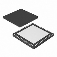
IC PIC MCU FLASH 128K 64-QFN
Manufacturer
Microchip Technology
Series
PIC® 24Fr
Datasheets
1.PIC24FJ128GA106-IPT.pdf
(14 pages)
2.PIC24FJ128GA106-IPT.pdf
(330 pages)
3.PIC24FJ128GA106-IPT.pdf
(52 pages)
4.PIC24FJ128GA110-EPT.pdf
(310 pages)
Specifications of PIC24FJ128GA106-E/MR
Program Memory Type
FLASH
Program Memory Size
128KB (43K x 24)
Package / Case
64-VFQFN, Exposed Pad
Core Processor
PIC
Core Size
16-Bit
Speed
32MHz
Connectivity
I²C, PMP, SPI, UART/USART
Peripherals
Brown-out Detect/Reset, POR, PWM, WDT
Number Of I /o
53
Ram Size
16K x 8
Voltage - Supply (vcc/vdd)
2 V ~ 3.6 V
Data Converters
A/D 16x10b
Oscillator Type
Internal
Operating Temperature
-40°C ~ 125°C
Processor Series
PIC24FJ
Core
PIC
Data Bus Width
16 bit
Data Ram Size
16 KB
Interface Type
I2C/SPI/UART
Maximum Clock Frequency
32 MHz
Number Of Programmable I/os
53
Number Of Timers
5
Maximum Operating Temperature
+ 125 C
Mounting Style
SMD/SMT
3rd Party Development Tools
52713-733, 52714-737, 53276-922, EWDSPIC
Development Tools By Supplier
PG164130, DV164035, DV244005, DV164005, PG164120, DM240001
Minimum Operating Temperature
- 40 C
On-chip Adc
16-ch x 10-bit
Lead Free Status / RoHS Status
Lead free / RoHS Compliant
Eeprom Size
-
Lead Free Status / Rohs Status
Lead free / RoHS Compliant


Silicon Errata Issues
1. Module: Core (RAM Operation)
2. Module: Core (BOR)
2010 Microchip Technology Inc.
Note:
If a RAM read is performed on the instruction
immediately prior to enabling Doze mode, an extra
read event may occur when Doze mode is
enabled. This has no effect on most SFRs and on
user RAM space. However, this could cause regis-
ters which also perform some action on a read
(such as auto-incrementing a pointer or removing
data from a FIFO buffer) to repeat that action,
possibly resulting in lost data or unexpected
operation.
Work around
Avoid reading registers which perform a second-
ary action (e.g., UART and SPI FIFO buffers, and
the RTCVAL registers) immediately prior to
entering Doze mode.
If this cannot be avoided, execute a NOP
instruction before entering Doze mode.
Affected Silicon Revisions
When the on-chip regulator is enabled (ENVREG
tied to V
occur under the following circumstances:
• V
• the internal band gap reference is being used as
• the CTMU module is enabled.
Work around
Limit the following activities to only those times
when the on-chip regulator is not in Tracking mode
(LVDIF (IFS4<8>) = 0):
• enabling the CTMU module;
• selecting the internal band gap as a reference
Affected Silicon Revisions
A3
A3
X
a reference with the A/D converter
(AD1PCFGH<1> or <0> = 0) or comparators
(CMxCON<1:0> = 11); or
for the A/D converter or the comparators.
X
DD
is less than 2.5V, and either:
This document summarizes all silicon
errata issues from all revisions of silicon,
previous as well as current. Only the
issues indicated by the shaded column in
the following tables apply to the current
silicon revision (A5).
A5
A5
X
DD
), a BOR event may spontaneously
PIC24FJ256GA110 FAMILY
3. Module: JTAG (Device Programming)
4
5. Module: I/O (PORTB)
The JTAGEN Configuration bit can be pro-
grammed to ‘0’ while using the JTAG interface for
device programming. This may cause a situation
where JTAG programming can lock itself out of
being able to program the device.
Work around
None.
Affected Silicon Revisions
Module: UART
When the UART is operating using two Stop bits
(STSEL = 1), it may sample the first Stop bit
instead of the second one. If the device being com-
municated with is one using one Stop bit in its
communications, this may lead to framing errors.
Work around
None.
Affected Silicon Revisions
When RB5 is configured as an open-drain output,
it remains in a high-impedance state. The settings
of LATB5 and TRISB5 have no effect on the pin’s
state.
Work around
If open-drain operation is not required, configure
RB5 as a regular I/O (ODCB<5> = 0).
If open-drain operation is required, there are two
options:
• select a different I/O pin for the open-drain
• place an external transistor on the pin, and
Affected Silicon Revisions
A3
A3
A3
function; or
configure the pin as a regular I/O.
X
X
X
A5
A5
A5
X
DS80368J-page 3
Related parts for PIC24FJ128GA106-E/MR
Image
Part Number
Description
Manufacturer
Datasheet
Request
R

Part Number:
Description:
General Purpose, 16-Bit Flash Microcontrollers
Manufacturer:
MICROCHIP [Microchip Technology]
Datasheet:

Part Number:
Description:
Manufacturer:
Microchip Technology Inc.
Datasheet:
Part Number:
Description:
Manufacturer:
Microchip Technology Inc.
Datasheet:
Part Number:
Description:
Manufacturer:
Microchip Technology Inc.
Datasheet:
Part Number:
Description:
Manufacturer:
Microchip Technology Inc.
Datasheet:
Part Number:
Description:
Manufacturer:
Microchip Technology Inc.
Datasheet:
Part Number:
Description:
Manufacturer:
Microchip Technology Inc.
Datasheet:
Part Number:
Description:
Manufacturer:
Microchip Technology Inc.
Datasheet:
Part Number:
Description:
Manufacturer:
Microchip Technology Inc.
Datasheet: