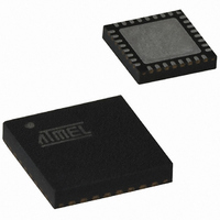
AT89C5131A-PUTUM Atmel, AT89C5131A-PUTUM Datasheet - Page 101

AT89C5131A-PUTUM
Manufacturer Part Number
AT89C5131A-PUTUM
Description
IC 8051 MCU FLASH 32K USB 32QFN
Manufacturer
Atmel
Series
AT89C513xr
Datasheet
1.AT89C5130A-PUTUM.pdf
(188 pages)
Specifications of AT89C5131A-PUTUM
Core Processor
C52X2
Core Size
8-Bit
Speed
48MHz
Connectivity
I²C, SPI, UART/USART, USB
Peripherals
LED, POR, PWM, WDT
Number Of I /o
18
Program Memory Size
32KB (32K x 8)
Program Memory Type
FLASH
Eeprom Size
4K x 8
Ram Size
1.25K x 8
Voltage - Supply (vcc/vdd)
2.7 V ~ 5.5 V
Oscillator Type
Internal
Operating Temperature
-40°C ~ 85°C
Package / Case
32-VQFN Exposed Pad, 32-HVQFN, 32-SQFN, 32-DHVQFN
Core
8051
Processor Series
AT89x
Data Bus Width
8 bit
Maximum Clock Frequency
48 MHz
Data Ram Size
1.25 KB
Number Of Programmable I/os
34
Number Of Timers
16 bit
Operating Supply Voltage
2.7 V to 5.5 V
Mounting Style
SMD/SMT
Height
0.95 mm
Interface Type
2-Wire, EUART, SPI, USB
Length
7 mm
Maximum Operating Temperature
+ 85 C
Minimum Operating Temperature
- 40 C
Supply Voltage (max)
5.5 V
Supply Voltage (min)
2.7 V
Width
7 mm
For Use With
AT89OCD-01 - USB EMULATOR FOR AT8XC51 MCUAT89STK-10 - KIT EVAL APPL MASS STORAGEAT89STK-05 - KIT STARTER FOR AT89C5131
Lead Free Status / RoHS Status
Lead free / RoHS Compliant
Data Converters
-
Lead Free Status / Rohs Status
Details
Available stocks
Company
Part Number
Manufacturer
Quantity
Price
Part Number:
AT89C5131A-PUTUM
Manufacturer:
ATMEL/爱特梅尔
Quantity:
20 000
- Current page: 101 of 188
- Download datasheet (2Mb)
19.3.5.3
4337K–USB–04/08
Serial Peripheral Data Register (SPDAT)
Reset Value = 00X0 XXXXb
Not Bit addressable
The Serial Peripheral Data Register
ter. A write to SPDAT places data directly into the shift register. No transmit buffer is available in
this model.
A Read of the SPDAT returns the value located in the receive buffer and not the content of the
shift register.
Table 19-5.
SPDAT - Serial Peripheral Data Register (0C5H)
Reset Value = Indeterminate
R7:R0: Receive data bits
SPCON, SPSTA and SPDAT registers may be read and written at any time while there is no on-
going exchange. However, special care should be taken when writing to them while a transmis-
sion is on-going:
Bit Number
• Do not change SPR2, SPR1 and SPR0
• Do not change CPHA and CPOL
• Do not change MSTR
• Clearing SPEN would immediately disable the peripheral
• Writing to the SPDAT will cause an overflow
R7
4
3
2
1
0
7
Mnemonic
SPDAT Register
MODF
Bit
R6
-
-
-
-
6
Description
Mode Fault
Cleared by hardware to indicate that the SS pin is at appropriate logic level, or has been
approved by a clearing sequence.
Set by hardware to indicate that the SS pin is at inappropriate logic level.
Reserved
The value read from this bit is indeterminate. Do not set this bit
Reserved
The value read from this bit is indeterminate. Do not set this bit
Reserved
The value read from this bit is indeterminate. Do not set this bit.
Reserved
The value read from this bit is indeterminate. Do not set this bit.
R5
5
(Table
R4
4
19-5) is a read/write buffer for the receive data regis-
R3
3
AT89C5130A/31A-M
R2
2
R1
1
R0
0
101
Related parts for AT89C5131A-PUTUM
Image
Part Number
Description
Manufacturer
Datasheet
Request
R

Part Number:
Description:
Manufacturer:
Atmel Corporation
Datasheet:

Part Number:
Description:
Manufacturer:
Atmel Corporation
Datasheet:

Part Number:
Description:
IC 8051 MCU FLASH 32K USB 52PLCC
Manufacturer:
Atmel
Datasheet:

Part Number:
Description:
IC MCU 32KB 3-3.6V USB 48-VQFN
Manufacturer:
Atmel
Datasheet:

Part Number:
Description:
MCU 8051 32K FLASH USB 28-SOIC
Manufacturer:
Atmel
Datasheet:

Part Number:
Description:
IC 8051 MCU FLASH 32K USB 64VQFP
Manufacturer:
Atmel
Datasheet:

Part Number:
Description:
MCU 8051 32K FLASH USB 64-VQFP
Manufacturer:
Atmel
Datasheet:

Part Number:
Description:
MCU 8051 32K FLASH USB 28-SOIC
Manufacturer:
Atmel
Datasheet:

Part Number:
Description:
MCU 8051 32K FLASH USB 52-PLCC
Manufacturer:
Atmel
Datasheet:

Part Number:
Description:
IC 8051 MCU FLASH 32K USB 48QFN
Manufacturer:
Atmel
Datasheet:

Part Number:
Description:
IC 8051 MCU FLASH 32K USB 64VQFP
Manufacturer:
Atmel
Datasheet:

Part Number:
Description:
IC 8051 MCU FLASH 32K USB 32QFN
Manufacturer:
Atmel
Datasheet:

Part Number:
Description:
IC 8051 MCU FLASH 32K USB 52PLCC
Manufacturer:
Atmel
Datasheet:

Part Number:
Description:
IC 8051 MCU FLASH 32K USB 28SOIC
Manufacturer:
Atmel
Datasheet:


