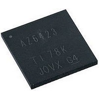
PIC18F67K22-I/MRRSL Microchip Technology, PIC18F67K22-I/MRRSL Datasheet - Page 167

PIC18F67K22-I/MRRSL
Manufacturer Part Number
PIC18F67K22-I/MRRSL
Description
MCU PIC 128K FLASH XLP 64QFN
Manufacturer
Microchip Technology
Series
PIC® XLP™ 18Fr
Datasheets
1.PIC16F722-ISS.pdf
(8 pages)
2.PIC18F65K22T-IPTRSL.pdf
(548 pages)
3.PIC18F65K22T-IPTRSL.pdf
(10 pages)
Specifications of PIC18F67K22-I/MRRSL
Core Size
8-Bit
Program Memory Size
128KB (64K x 16)
Core Processor
PIC
Speed
64MHz
Connectivity
I²C, LIN, SPI, UART/USART
Peripherals
Brown-out Detect/Reset, LVD, POR, PWM, WDT
Number Of I /o
53
Program Memory Type
FLASH
Eeprom Size
1K x 8
Ram Size
4K x 8
Voltage - Supply (vcc/vdd)
1.8 V ~ 5.5 V
Data Converters
A/D 16x12b
Oscillator Type
Internal
Operating Temperature
-40°C ~ 85°C
Package / Case
64-VFQFN, Exposed Pad
Controller Family/series
PIC18
Eeprom Memory Size
1024Byte
Ram Memory Size
3862Byte
Cpu Speed
16MIPS
No. Of Timers
11
Processor Series
PIC18F
Core
PIC
Data Bus Width
8 bit
Data Ram Size
4 KB
Interface Type
I2C, SPI, EUSART
Maximum Clock Frequency
64 MHz
Number Of Programmable I/os
53
Number Of Timers
11
Operating Supply Voltage
1.8 V to 5.5 V
Maximum Operating Temperature
+ 85 C
Mounting Style
SMD/SMT
3rd Party Development Tools
52715-96, 52716-328, 52717-734, 52712-325, EWPIC18
Development Tools By Supplier
DM180021, DM183026-2, DM183032, DV164131, MA180028
Minimum Operating Temperature
- 40 C
On-chip Adc
12 bit, 16 Channel
Lead Free Status / RoHS Status
Lead free / RoHS Compliant
Lead Free Status / RoHS Status
Lead free / RoHS Compliant
Available stocks
Company
Part Number
Manufacturer
Quantity
Price
Company:
Part Number:
PIC18F67K22-I/MRRSL
Manufacturer:
FSC
Quantity:
250
- PIC16F722-ISS PDF datasheet
- PIC18F65K22T-IPTRSL PDF datasheet #2
- PIC18F65K22T-IPTRSL PDF datasheet #3
- Current page: 167 of 548
- Download datasheet (5Mb)
REGISTER 12-4:
12.1.4
Many of the ports multiplex analog and digital function-
ality, providing a lot of flexibility for hardware designers.
PIC18F87K22 family devices can make any analog pin
analog or digital, depending on an application’s needs.
The ports’ analog/digital functionality is controlled by
the registers: ANCON0, ANCON1 and ANCON2.
2010 Microchip Technology Inc.
bit 7
Legend:
R = Readable bit
-n = Value at POR
bit 7
bit 6
bit 5-1
bit 0
R/W-0
U2OD
ANALOG AND DIGITAL PORTS
U2OD: EUSART2 Open-Drain Output Enable bit
1 = Open-drain capability enabled
0 = Open-drain capability disabled
U1OD: EUSART1 Open-Drain Output Enable bit
1 = Open-drain capability enabled
0 = Open-drain capability disabled
Unimplemented: Read as ‘0’
CTMUDS: CTMU Pulse Delay Enable bit
1 = Pulse delay input for CTMU enabled on pin, RF1
0 = Pulse delay input for CTMU disabled on pin, RF1
R/W-0
U1OD
ODCON3: PERIPHERAL OPEN-DRAIN CONTROL REGISTER 3
W = Writable bit
‘1’ = Bit is set
U-0
—
U-0
Preliminary
—
U = Unimplemented bit, read as ‘0’
‘0’ = Bit is cleared
PIC18F87K22 FAMILY
Setting these registers makes the corresponding pins
analog and clearing the registers makes the ports digi-
tal. For details on these registers, see Section 23.0
“12-Bit Analog-to-Digital Converter (A/D) Module”
U-0
—
U-0
—
x = Bit is unknown
U-0
—
DS39960B-page 167
CTMUDS
R/W-0
bit 0
Related parts for PIC18F67K22-I/MRRSL
Image
Part Number
Description
Manufacturer
Datasheet
Request
R

Part Number:
Description:
MCU PIC 128K FLASH XLP 64TQFP
Manufacturer:
Microchip Technology
Datasheet:

Part Number:
Description:
128kB Flash, 4kB RAM, 1kB EE, NanoWatt XLP, GP 64 QFN 9x9x0.9mm TUBE
Manufacturer:
Microchip Technology
Datasheet:

Part Number:
Description:
128kB Flash, 4kB RAM, 1kB EE, NanoWatt XLP, GP 64 TQFP 10x10x1mm TRAY
Manufacturer:
Microchip Technology
Datasheet:

Part Number:
Description:
128kB Flash, 4kB RAM, 1kB EE, NanoWatt XLP, GP 64 QFN 9x9x0.9mm TUBE
Manufacturer:
Microchip Technology
Datasheet:

Part Number:
Description:
128kB Flash, 4kB RAM, 1kB EE, NanoWatt XLP, GP 64 TQFP 10x10x1mm TRAY
Manufacturer:
Microchip Technology

Part Number:
Description:
Manufacturer:
Microchip Technology Inc.
Datasheet:

Part Number:
Description:
Manufacturer:
Microchip Technology Inc.
Datasheet:

Part Number:
Description:
Manufacturer:
Microchip Technology Inc.
Datasheet:

Part Number:
Description:
Manufacturer:
Microchip Technology Inc.
Datasheet:

Part Number:
Description:
Manufacturer:
Microchip Technology Inc.
Datasheet:

Part Number:
Description:
Manufacturer:
Microchip Technology Inc.
Datasheet:


