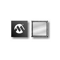
PIC18F47J53-I/ML Microchip Technology, PIC18F47J53-I/ML Datasheet - Page 351

PIC18F47J53-I/ML
Manufacturer Part Number
PIC18F47J53-I/ML
Description
IC PIC MCU 128KB FLASH 44QFN
Manufacturer
Microchip Technology
Series
PIC® XLP™ 18Fr
Datasheets
1.PIC18LF24J10-ISS.pdf
(32 pages)
2.PIC18F26J13-ISS.pdf
(496 pages)
3.PIC18F26J53-ISS.pdf
(586 pages)
4.PIC18F26J53-ISS.pdf
(12 pages)
Specifications of PIC18F47J53-I/ML
Program Memory Type
FLASH
Program Memory Size
128KB (64K x 16)
Package / Case
*
Core Processor
PIC
Core Size
8-Bit
Speed
48MHz
Connectivity
I²C, LIN, SPI, UART/USART, USB
Peripherals
Brown-out Detect/Reset, POR, PWM, WDT
Number Of I /o
34
Ram Size
3.8K x 8
Voltage - Supply (vcc/vdd)
2.15 V ~ 3.6 V
Data Converters
A/D 13x10b/12b
Oscillator Type
Internal
Operating Temperature
-40°C ~ 85°C
Processor Series
PIC18F
Core
PIC
Data Bus Width
8 bit
Data Ram Size
3.8 KB
Interface Type
I2C, SPI, USART
Maximum Clock Frequency
48 MHz
Number Of Programmable I/os
22
Number Of Timers
8
Operating Supply Voltage
2.15 V to 3.6 V
Maximum Operating Temperature
+ 85 C
Mounting Style
SMD/SMT
3rd Party Development Tools
52715-96, 52716-328, 52717-734, 52712-325, EWPIC18
Minimum Operating Temperature
- 40 C
Controller Family/series
PIC18
Cpu Speed
48MHz
Embedded Interface Type
I2C, SPI, USART
Digital Ic Case Style
QFN
Supply Voltage Range
1.8V To 5.5V
Rohs Compliant
Yes
Lead Free Status / RoHS Status
Lead free / RoHS Compliant
For Use With
MA180029 - BOARD DEMO PIC18F47J53 FS USB
Eeprom Size
-
Lead Free Status / Rohs Status
Lead free / RoHS Compliant
Available stocks
Company
Part Number
Manufacturer
Quantity
Price
Company:
Part Number:
PIC18F47J53-I/ML
Manufacturer:
MICROCHIP
Quantity:
1 100
- PIC18LF24J10-ISS PDF datasheet
- PIC18F26J13-ISS PDF datasheet #2
- PIC18F26J53-ISS PDF datasheet #3
- PIC18F26J53-ISS PDF datasheet #4
- Current page: 351 of 496
- Download datasheet (5Mb)
REGISTER 24-1:
2010 Microchip Technology Inc.
bit 7
Legend:
R = Readable bit
-n = Value when device is unprogrammed
bit 7
bit 6
bit 5
bit 4
bit 3-0
Note 1:
R/P-0
IESO
When FOSC<3:0> is configured for HS, XT, or LP oscillator and FCMEN bit is set, then the IESO bit
should also be set to prevent a false failed clock indication and to enable automatic clock switch over from
the internal oscillator block to the external oscillator when the OST times out.
IESO
1 = Oscillator Switchover mode enabled
0 = Oscillator Switchover mode disabled
FCMEN
1 = Fail-Safe Clock Monitor enabled
0 = Fail-Safe Clock Monitor disabled
PRICLKEN: Primary Clock Enable bit
1 = Primary Clock is always enabled
0 = Primary Clock can be disabled by software
PLLCFG: 4 x PLL Enable bit
1 = 4 x PLL always enabled, Oscillator multiplied by 4
0 = 4 x PLL is under software control, PLLEN (OSCTUNE<6>)
FOSC<3:0>: Oscillator Selection bits
1111 = External RC oscillator, CLKOUT function on RA6
1110 = External RC oscillator, CLKOUT function on RA6
1101 = EC oscillator (low power, <500 kHz)
1100 = EC oscillator, CLKOUT function on OSC2 (low power, <500 kHz)
1011 = EC oscillator (medium power, 500 kHz-16 MHz)
1010 = EC oscillator, CLKOUT function on OSC2 (medium power, 500 kHz-16 MHz)
1001 = Internal oscillator block, CLKOUT function on OSC2
1000 = Internal oscillator block
0111 = External RC oscillator
0110 = External RC oscillator, CLKOUT function on OSC2
0101 = EC oscillator (high power, >16 MHz)
0100 = EC oscillator, CLKOUT function on OSC2 (high power, >16 MHz)
0011= HS oscillator (medium power, 4 MHz-16 MHz)
0010= HS oscillator (high power, >16 MHz)
0001= XT oscillator
0000= LP oscillator
FCMEN
R/P-0
(1)
CONFIG1H: CONFIGURATION REGISTER 1 HIGH
: Internal/External Oscillator Switchover bit
(1)
: Fail-Safe Clock Monitor Enable bit
P = Programmable bit
PRICLKEN
R/P-1
PLLCFG
R/P-0
Preliminary
U = Unimplemented bit, read as ‘0’
x = Bit is unknown
R/P-0
PIC18(L)F2X/4XK22
R/P-1
FOSC<3:0>
R/P-0
DS41412D-page 351
R/P-1
bit 0
Related parts for PIC18F47J53-I/ML
Image
Part Number
Description
Manufacturer
Datasheet
Request
R

Part Number:
Description:
Manufacturer:
Microchip Technology Inc.
Datasheet:

Part Number:
Description:
Manufacturer:
Microchip Technology Inc.
Datasheet:

Part Number:
Description:
Manufacturer:
Microchip Technology Inc.
Datasheet:

Part Number:
Description:
Manufacturer:
Microchip Technology Inc.
Datasheet:

Part Number:
Description:
Manufacturer:
Microchip Technology Inc.
Datasheet:

Part Number:
Description:
Manufacturer:
Microchip Technology Inc.
Datasheet:

Part Number:
Description:
Manufacturer:
Microchip Technology Inc.
Datasheet:

Part Number:
Description:
Manufacturer:
Microchip Technology Inc.
Datasheet:


