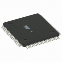
ATMEGA6490A-AU Atmel, ATMEGA6490A-AU Datasheet - Page 23

ATMEGA6490A-AU
Manufacturer Part Number
ATMEGA6490A-AU
Description
IC MCU AVR 64K FLASH 100TQFP
Manufacturer
Atmel
Series
AVR® ATmegar
Specifications of ATMEGA6490A-AU
Core Processor
AVR
Core Size
8-Bit
Speed
20MHz
Connectivity
SPI, UART/USART, USI
Peripherals
Brown-out Detect/Reset, LCD, POR, PWM, WDT
Number Of I /o
69
Program Memory Size
64KB (32K x 16)
Program Memory Type
FLASH
Eeprom Size
2K x 8
Ram Size
4K x 8
Voltage - Supply (vcc/vdd)
1.8 V ~ 5.5 V
Data Converters
A/D 8x10b
Oscillator Type
Internal
Operating Temperature
-40°C ~ 85°C
Package / Case
100-TFQFP
Processor Series
ATmega
Core
AVR
Data Bus Width
8 bit
Data Ram Size
4 KB
Interface Type
SPI, USART
Maximum Clock Frequency
20 MHz
Number Of Programmable I/os
69
Number Of Timers
3
Operating Supply Voltage
3.3 V
Maximum Operating Temperature
+ 85 C
Mounting Style
SMD/SMT
Minimum Operating Temperature
- 40 C
Operating Temperature Range
- 40 C to + 85 C
Lead Free Status / RoHS Status
Lead free / RoHS Compliant
Available stocks
Company
Part Number
Manufacturer
Quantity
Price
Company:
Part Number:
ATMEGA6490A-AU
Manufacturer:
Atmel
Quantity:
1 250
Company:
Part Number:
ATMEGA6490A-AUR
Manufacturer:
Maxim
Quantity:
43
- Current page: 23 of 712
- Download datasheet (41Mb)
8284A–AVR–10/10
1. Wait until EEWE becomes zero.
2. Wait until SPMEN in SPMCSR becomes zero.
3. Write new EEPROM address to EEAR (optional).
4. Write new EEPROM data to EEDR (optional).
5. Write a logical one to the EEMWE bit while writing a zero to EEWE in EECR.
6. Within four clock cycles after setting EEMWE, write a logical one to EEWE.
The EEPROM can not be programmed during a CPU write to the Flash memory. The software
must check that the Flash programming is completed before initiating a new EEPROM write.
Step 2 is only relevant if the software contains a Boot Loader allowing the CPU to program the
Flash. If the Flash is never being updated by the CPU, step 2 can be omitted. See
Support – Read-While-Write Self-Programming” on page 295
programming.
Caution: An interrupt between step 5 and step 6 will make the write cycle fail, since the
EEPROM Master Write Enable will time-out. If an interrupt routine accessing the EEPROM is
interrupting another EEPROM access, the EEAR or EEDR Register will be modified, causing the
interrupted EEPROM access to fail. It is recommended to have the Global Interrupt Flag cleared
during all the steps to avoid these problems.
When the write access time has elapsed, the EEWE bit is cleared by hardware. The user soft-
ware can poll this bit and wait for a zero before writing the next byte. When EEWE has been set,
the CPU is halted for two cycles before the next instruction is executed.
The user should poll the EEWE bit before starting the read operation. If a write operation is in
progress, it is neither possible to read the EEPROM, nor to change the EEAR Register.
The calibrated Oscillator is used to time the EEPROM accesses.
gramming time for EEPROM access from the CPU.
Table 7-1.
The following code examples show one assembly and one C function for writing to the
EEPROM. To avoid that interrupts will occur during execution of these functions, the examples
assume that interrupts are controlled (e.g. by disabling interrupts globally). The examples also
assume that no Flash Boot Loader is present in the software. If such code is present, the
EEPROM write function must also wait for any ongoing SPM command to finish.
Symbol
EEPROM write (from CPU)
ATmega169A/169PA/329A/329PA/649A/649P/3290A/3290PA/6490A/6490P
EEPROM Programming Time
Number of Calibrated
RC Oscillator Cycles
27 072
Table 7-1
Typical Programming Time
for details about Boot
lists the typical pro-
3.3 ms
”Boot Loader
23
Related parts for ATMEGA6490A-AU
Image
Part Number
Description
Manufacturer
Datasheet
Request
R

Part Number:
Description:
Manufacturer:
Atmel Corporation
Datasheet:

Part Number:
Description:
IC AVR MCU FLASH 64K 64-QFN
Manufacturer:
Atmel
Datasheet:

Part Number:
Description:
IC AVR MCU FLASH 64K 64TQFP
Manufacturer:
Atmel
Datasheet:

Part Number:
Description:
IC AVR MCU FLASH 64K 5V 64TQFP
Manufacturer:
Atmel
Datasheet:

Part Number:
Description:
IC AVR MCU FLASH 64K 5V 64QFN
Manufacturer:
Atmel
Datasheet:

Part Number:
Description:
MCU AVR 64KB FLASH 16MHZ 64QFN
Manufacturer:
Atmel
Datasheet:

Part Number:
Description:
IC MCU AVR FLASH 64K 64TQFP
Manufacturer:
Atmel
Datasheet:

Part Number:
Description:
Manufacturer:
Atmel Corporation
Datasheet:

Part Number:
Description:
Manufacturer:
ATMEL Corporation
Datasheet:

Part Number:
Description:
Manufacturer:
ATMEL Corporation
Datasheet:

Part Number:
Description:
IC AVR MCU 64K 16MHZ 5V 64TQFP
Manufacturer:
Atmel
Datasheet:

Part Number:
Description:
IC AVR MCU 64K 16MHZ 5V 64-QFN
Manufacturer:
Atmel
Datasheet:

Part Number:
Description:
IC AVR MCU 64K 16MHZ COM 64-TQFP
Manufacturer:
Atmel
Datasheet:

Part Number:
Description:
IC AVR MCU 64K 16MHZ IND 64-TQFP
Manufacturer:
Atmel
Datasheet:

Part Number:
Description:
IC AVR MCU 64K 16MHZ COM 64-QFN
Manufacturer:
Atmel
Datasheet:


