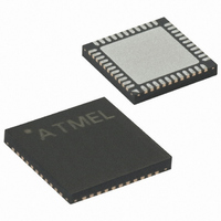
ATMEGA644PA-MU Atmel, ATMEGA644PA-MU Datasheet - Page 272

ATMEGA644PA-MU
Manufacturer Part Number
ATMEGA644PA-MU
Description
IC MCU 8BIT 64KB FLASH 44VQFN
Manufacturer
Atmel
Series
AVR® ATmegar
Specifications of ATMEGA644PA-MU
Core Processor
AVR
Core Size
8-Bit
Speed
20MHz
Connectivity
I²C, SPI, UART/USART
Peripherals
Brown-out Detect/Reset, POR, PWM, WDT
Number Of I /o
32
Program Memory Size
64KB (32K x 16)
Program Memory Type
FLASH
Eeprom Size
2K x 8
Ram Size
4K x 8
Voltage - Supply (vcc/vdd)
1.8 V ~ 5.5 V
Data Converters
A/D 8x10b
Oscillator Type
Internal
Operating Temperature
-40°C ~ 85°C
Package / Case
44-VQFN Exposed Pad
Processor Series
ATMEGA64x
Core
AVR8
Data Bus Width
8 bit
Data Ram Size
4 KB
Interface Type
SPI, TWI, UART
Maximum Clock Frequency
20 MHz
Number Of Programmable I/os
32
Operating Supply Voltage
1.8 V to 5.5 V
Maximum Operating Temperature
+ 85 C
Mounting Style
SMD/SMT
3rd Party Development Tools
EWAVR, EWAVR-BL
Development Tools By Supplier
ATAVRDRAGON, ATSTK500, ATSTK600, ATAVRISP2, ATAVRONEKIT
Minimum Operating Temperature
- 40 C
Lead Free Status / RoHS Status
Lead free / RoHS Compliant
Available stocks
Company
Part Number
Manufacturer
Quantity
Price
Company:
Part Number:
ATMEGA644PA-MU
Manufacturer:
ATMEL
Quantity:
5 600
Part Number:
ATMEGA644PA-MU
Manufacturer:
ATMEL/爱特梅尔
Quantity:
20 000
- Current page: 272 of 581
- Download datasheet (27Mb)
24.5.2
8272A–AVR–01/10
Scanning the RESET Pin
Figure 24-4. General Port Pin Schematic Diagram
The RESET pin accepts 5V active low logic for standard reset operation, and 12V active high
logic for High Voltage Parallel programming. An observe-only cell as shown in
inserted for the 5V reset signal.
Figure 24-5. Observe-only Cell
164A/164PA/324A/324PA/644A/644PA/1284/1284P
See Boundary-scan
Description for Details!
Pxn
From System Pin
PUD:
PUExn:
OCxn:
ODxn:
IDxn:
SLEEP:
IDxn
PULLUP DISABLE
PULLUP ENABLE for pin Pxn
OUTPUT CONTROL for pin Pxn
OUTPUT DATA to pin Pxn
INPUT DATA from pin Pxn
SLEEP CONTROL
Previous
From
PUExn
Cell
ShiftDR
0
1
ClockDR
SLEEP
OCxn
ODxn
D
FF1
SYNCHRONIZER
WDx:
RDx:
WRx:
RRx:
RPx:
CLK
D
L
Q
Q
Q
Next
I/O
Cell
To
:
D
WRITE DDRx
READ DDRx
WRITE PORTx
READ PORTx REGISTER
READ PORTx PIN
I/O CLOCK
PINxn
Q
Q
To System Logic
RESET
RESET
Q
Q
Q
Q
PORTxn
DDxn
CLR
CLR
D
D
CLK
PUD
WDx
RDx
WRx
RPx
RRx
I/O
Figure 24-5
272
is
Related parts for ATMEGA644PA-MU
Image
Part Number
Description
Manufacturer
Datasheet
Request
R

Part Number:
Description:
Manufacturer:
Atmel Corporation
Datasheet:

Part Number:
Description:
IC AVR MCU FLASH 64K 44-QFN
Manufacturer:
Atmel
Datasheet:

Part Number:
Description:
IC AVR MCU FLASH 64K 44TQFP
Manufacturer:
Atmel
Datasheet:

Part Number:
Description:
IC AVR MCU FLASH 64K 40DIP
Manufacturer:
Atmel
Datasheet:

Part Number:
Description:
MCU AVR 64K FLASH 20MHZ 44TQFP
Manufacturer:
Atmel
Datasheet:

Part Number:
Description:
MCU AVR 64K FLASH 20MHZ 44QFN
Manufacturer:
Atmel
Datasheet:

Part Number:
Description:
Atmega644 8-bit Avr Microcontroller With 64k Bytes In-system Programmable Flash
Manufacturer:
ATMEL Corporation
Datasheet:

Part Number:
Description:
Manufacturer:
Atmel Corporation
Datasheet:

Part Number:
Description:
Manufacturer:
ATMEL Corporation
Datasheet:

Part Number:
Description:
Manufacturer:
ATMEL Corporation
Datasheet:

Part Number:
Description:
IC AVR MCU 64K 16MHZ 5V 64TQFP
Manufacturer:
Atmel
Datasheet:

Part Number:
Description:
IC AVR MCU 64K 16MHZ 5V 64-QFN
Manufacturer:
Atmel
Datasheet:


