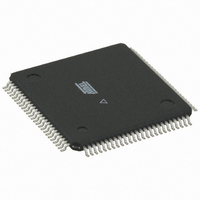
ATMEGA1280-16AUR Atmel, ATMEGA1280-16AUR Datasheet - Page 32

ATMEGA1280-16AUR
Manufacturer Part Number
ATMEGA1280-16AUR
Description
MCU AVR 128K FLASH 16MHZ 100TQFP
Manufacturer
Atmel
Series
AVR® ATmegar
Specifications of ATMEGA1280-16AUR
Core Processor
AVR
Core Size
8-Bit
Speed
16MHz
Connectivity
EBI/EMI, I²C, SPI, UART/USART
Peripherals
Brown-out Detect/Reset, POR, PWM, WDT
Number Of I /o
86
Program Memory Size
128KB (64K x 16)
Program Memory Type
FLASH
Eeprom Size
4K x 8
Ram Size
8K x 8
Voltage - Supply (vcc/vdd)
2.7 V ~ 5.5 V
Data Converters
A/D 16x10b
Oscillator Type
Internal
Operating Temperature
-40°C ~ 85°C
Package / Case
100-TQFP, 100-VQFP
For Use With
ATSTK600-TQFP100 - STK600 SOCKET/ADAPTER 100-TQFPATSTK503 - STARTER KIT AVR EXP MODULE 100P
Lead Free Status / RoHS Status
Lead free / RoHS Compliant
Available stocks
Company
Part Number
Manufacturer
Quantity
Price
- Current page: 32 of 444
- Download datasheet (10Mb)
8.1.5
2549M–AVR–09/10
Using all Locations of External Memory Smaller than 64 Kbytes
Figure 8-5.
Note:
Figure 8-6.
Note:
Since the external memory is mapped after the internal memory as shown in
28, the external memory is not addressed when addressing the first 8,704 bytes of data space. It
may appear that the first 8,704 bytes of the external memory are inaccessible (external memory
addresses 0x0000 to 0x21FF). However, when connecting an external memory smaller than 64
Kbytes, for example 32 Kbytes, these locations are easily accessed simply by addressing from
address 0x8000 to 0xA1FF. Since the External Memory Address bit A15 is not connected to the
external memory, addresses 0x8000 to 0xA1FF will appear as addresses 0x0000 to 0x21FF for
the external memory. Addressing above address 0xA1FF is not recommended, since this will
address an external memory location that is already accessed by another (lower) address. To
System Clock (CLK
System Clock (CLK
DA7:0 (XMBK = 0)
DA7:0 (XMBK = 1)
DA7:0 (XMBK = 0)
DA7:0 (XMBK = 1)
1. SRWn1 = SRW11 (upper sector) or SRW01 (lower sector), SRWn0 = SRW10 (upper sector) or
1. SRWn1 = SRW11 (upper sector) or SRW01 (lower sector), SRWn0 = SRW10 (upper sector) or
SRW00 (lower sector).
The ALE pulse in period T6 is only present if the next instruction accesses the RAM (internal
or external).
SRW00 (lower sector).
The ALE pulse in period T7 is only present if the next instruction accesses the RAM (internal
or external).
DA7:0
A15:8
CPU
ALE
DA7:0
WR
A15:8
RD
External Data Memory Cycles with SRWn1 = 1 and SRWn0 = 0
External Data Memory Cycles with SRWn1 = 1 and SRWn0 = 1
CPU
ALE
WR
)
RD
)
Prev. addr.
Prev. data
Prev. data
Prev. data
Prev. addr.
Prev. data
Prev. data
Prev. data
T1
T1
Address
Address
Address
ATmega640/1280/1281/2560/2561
T2
Address
Address
Address
XX
T2
XX
Address
T3
Data
Data
Data
Address
T3
Data
Data
Data
T4
T4
T5
T5
T6
Figure 8-1 on page
(1)
(1)
T6
T7
32
Related parts for ATMEGA1280-16AUR
Image
Part Number
Description
Manufacturer
Datasheet
Request
R

Part Number:
Description:
Manufacturer:
Atmel Corporation
Datasheet:

Part Number:
Description:
IC MCU AVR 128K FLASH 100-CBGA
Manufacturer:
Atmel
Datasheet:

Part Number:
Description:
IC MCU AVR 128K FLASH 100-TQFP
Manufacturer:
Atmel
Datasheet:

Part Number:
Description:
MCU AVR 128K FLASH 16MHZ 100CBGA
Manufacturer:
Atmel
Datasheet:

Part Number:
Description:
Manufacturer:
ATMEL Corporation
Datasheet:

Part Number:
Description:
Microcontroller with 128K bytes In-system programmable flash, 8 MHz, power supply =2.7 - 5.5V
Manufacturer:
ATMEL Corporation
Datasheet:

Part Number:
Description:
IC AVR MCU 128K 16MHZ 5V 64TQFP
Manufacturer:
Atmel
Datasheet:

Part Number:
Description:
IC AVR MCU 128K 16MHZ 5V 64-QFN
Manufacturer:
Atmel
Datasheet:

Part Number:
Description:
IC AVR MCU 128K 16MHZ COM 64-QFN
Manufacturer:
Atmel
Datasheet:

Part Number:
Description:
IC AVR MCU 128K 16MHZ 64-TQFP
Manufacturer:
Atmel
Datasheet:

Part Number:
Description:
IC AVR MCU 128K 16MHZ 64-TQFP
Manufacturer:
Atmel
Datasheet:


